ISO 7816 smartcard interface monitor
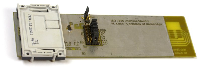
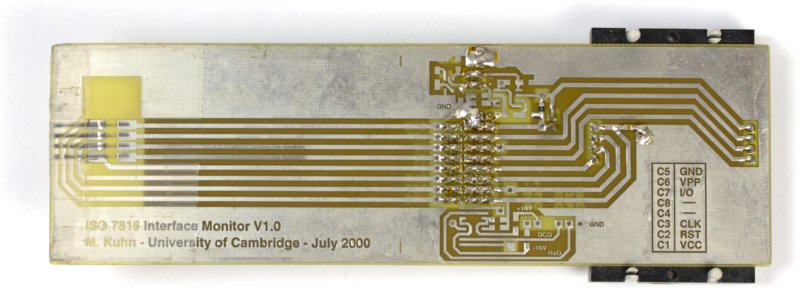
In July 2000, I produced a little printed-circuit-board adapter to help in experiments involving the ISO 7816 contact smartcard interface. At one end, this little PCB has the shape of an ISO 7816 smartcard, including all eight contacts. The other end can be fitted with a smartcard connector. All eight pins of the smartcard end and the card connector end are linked via a row of jumpers and have test pins. This way, the device can be used in pass-through mode, to passively eavesdrop on ISO 7816 smartcard data traffic, or you can open each line and pass it via external electronics, which then can interfere in real-time with the smartcard communication. You can also just use one end at a time, to build either a smartcard interface or a card emulator.
The device also can be fitted with a current-sensing SMD resistor (~10 Ω) in the ground line of the smartcard contact, such that it can be used for power-analysis attack on smartcards, and an SMD capacitor across the card-interface power supply.
This little adapter card has seen a lot of action in many smartcard related research projects at the department's Security Group. Most famously, my former PhD students Steven Murdoch and Saar Drimer used it to demonstrate several serious defects in the Chip & PIN (EMV) banking card protocol, and in this context it was seen several times on TV.
Technical details
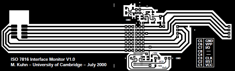
Rather than using specialized PCB layout software, I simply drew the layout of this simple board using a normal vector drawing program, the Unix/X11 classic xfig. The drawing can be laser printed onto a transparency. Make two copies and place one onto each side of an A4-sized PCB covered on both sides with copper and photoresist. This will result in four adapter boards.
Make sure you use 0.8 mm thick PCB material, which is about half the thickness of regular PCBs. The ISO 7816 smartcard defines the card to be 0.76 mm thick, and 0.8 mm works just as well, but anything much thicker is unlikely to fit into many smartcard slots.
The design can be produced as a single-sided or double-sided board. As a double-sided board, you get a ground plane on top (good EMC practice) along with labels next to the test pins.
Note: The adapter also has space for adding a few more optional components, namely (a) a buffer amplifier for the current-sense voltage, and an associated DC-DC power-supply converter, and (b) a chip to convert between TTL and RS-232 levels to, an old trick to build a very simple smartcard emulator. See README.txt for details on the intended components. We've never actually populated those places. Regarding the amplifier, it is much easier to get excellent power-analysis signals merely by using a very short (~10 cm) coax cable directly into the port of a digital storage oscilloscope. Regarding the trick of using a voltage converter to connect to an RS-232 port, that only works with certain clock frequencies, and while it was practical on some early pay-TV set-top boxes, it was not with many EMV terminals, where we had to implement a UART clocked by the card interface on a separate FPGA board.
Practical tips
- Be careful when printing PDFs from Adobe Reader, which by default rescales every PDF it prints onto the printable area of your printer, which is usually a bit smaller than the full A4 size of 297 × 210 mm! Make sure to switch off any scaling in the Print dialog box of Adobe Reader when printing transparencies for making PCBs. (Or even better, cut out the PDF step and send the provided PostScript files directly to you PostScript printer.)
- If you use the laser printed transparencies, use the reversed an inverted version of the file, such that you can put the toner side directly onto the photo resist, and such that only the parts where you want to remove copper are exposed.
- On the smartcard contact side, the front centimetre or so is meant to be covered with some insulating film (e.g., sticky tape), to avoid wiping contacts touching any of the conductive parts of the PCB when it is inserted into a smartcard interface.
Files
- Xfig file
- Normal: PostScript, PDF
- Reversed and inverted: PostScript, PDF
- README.txt
Creative Commons Attribution
4.0 International License.
