ECAD and Architecture Practical Classes
Verilog Tutorial Part 3 - State Machines
Revision: state machines
Most commonly we will use simple Moore state machines (see the Wikipedia entry or the Digital Electronics course for details). A simple Moore state machine is depicted below. The outputs are derived directly from registers. The combinational function (f in the figure) computes the next state including the outputs. A bank of (one or more) D flip-flops (DFFs) passes the next state value through to the outputs on the clock edge (often the rising edge), otherwise they remember/hold their state.
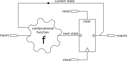
Simple Moore state machine
Notes:
- There can be zero or many inputs
- There can be one or many outputs (zero outputs is rather pointless!)
- The current state may be some or all of the outputs
- The bits sent to the output and current state may or may not be disjoint.
Sometimes it is useful to add a combinational function (g in the figure below) to derive the final output. You will use this form for Tick 2 - Traffic Lights.
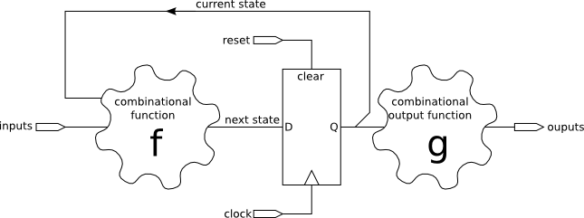
Moore state machine with function on output
The other alternative is the Mealy machine which includes a direct path from some or all of the inputs to the outputs.
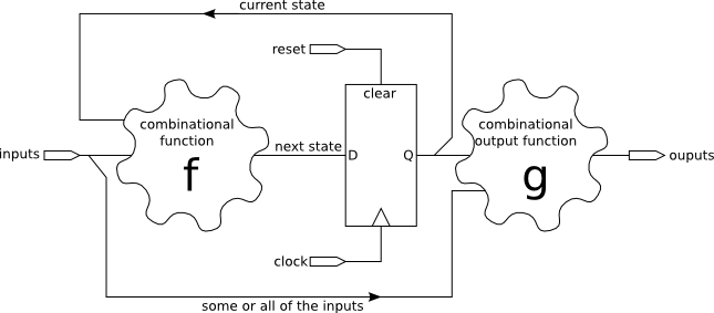
Mealy state machine
To implement state machines we need to be able to describe the use of
DFFs, so lets do this next.
Registers
So far we have designed combinational circuits and wrapped them into modules, but to produce more interesting designs we need to be able to describe state machines. In order to describe state machines we need to instantiate state holding elements. A very common approach (which is supported by the FPGAs) is to use D flip-flops (DFFs) which have the following circuit symbol:

D flip-flop circuit element
As you will know from the first year Digital Electronics course, DFFs have the following behaviour:
| clock | clear | D | Q' | |
| X | 1 | X | 0 | |
| 0 | 0 | X | Q | |
| 1 | 0 | X | Q | |
 | 0 | 0 | 0 | |
| 0 | 1 | 1 |
Where Q' is the new value of the output and Q is the current value of the output.
From the early days of Verilog (which predates SystemVerilog), registers have been declared viz:
reg r;
If we read from register r then we implicitly refer to the Q output of the DFF and writes refer to the D input. But we need a notation to connect the clock and (optionally) reset signals. SystemVerilog uses the following notation:
always_ff @(posedge clock or posedge reset)
  if(reset)
    r <= 0;
  else
    r <= !r;
Let's unpick this example:
always_ff- always perform the following actions whenever the sensitivity list (the bit in parentheses) is true. The_ffsuffix is new to SystemVerilog and indicates that all assignments inside the always need to be to registers and not wires. For SystemVerilog code synthesised to a circuit, the sensitivity list foralways_ffis just for clock and reset, with these signals being directly wired to the DFFs. Tutorial 4 talks about SystemVerilog test bench code that is not synthesisable but instead is used to test a design in simulation.@(posedge clock or posedge reset)- is the sensitivity list which will be true whenever there is a rising edge for theclockor a rising edge onresetif(reset)- detects whenreset==1. Note that this is the standard form for an asynchronous reset. Despite theposedge resetin thealways_ffsensitivity list suggesting that the reset is at the positive edge, the reset will in fact be level sensitive and asynchronous (i.e. independent of the clock)r <= !r;causes r to toggle every clock edge. Normally we put some much more interesting code here manipulating far more state bits. The assignment operator<=is called non-blocking assignment which results in all assignments being performed in parallel at the clock edge, i.e. just like real circuits which are inherently parallel.
Logics, wires and registers
SystemVerilog adds the logic type on top of Verilog's reg and wire.
How do they differ?
Verilog has two kinds of data types.
Nets provide connectivity: the signal connecting two logic gates (as in the full adder example) holds no state.
For this purpose wire is used. Wires have no memory and need to be continuously driven (although they can be driven to a value of x meaning 'undefined').
Variables represent storage of state over time. For example, a flip-flop is a state-holding element.
Until the state is changed they will always retain their current state.
Verilog defined the reg type to represent this.
However, Verilog defines behaviour by use rather than by type and so the names of types can be misleading: a reg can also be used for combinational nets:
// combinational adder
input [7:0] a;
input [7:0] b;
reg [7:0] result;
assign result = a + b;
For this reason, SystemVerilog provides logic as an alternative to
reg and wire. It is then inferred
whether a logic variable is actually a net or a variable depending on
whether it is used in an always_comb (i.e. combinational block - more below) or
always_ff block (i.e. a state-machine or flip-flop block).
In practice reg and logic behave the same; the type is simply renamed for clarity.
Memories
Memories can be described as an array of registers in the following manner:
reg [DATA_WIDTH-1:0] myram [0:MEM_SIZE-1];
Memories can be made out of lots of DFFs, but this is an inefficient implementation. FPGAs provide lots of embedded memories called Block RAM or BRAM. BRAMs on Altera FPGAs can be used in various forms, but a common form is to have two ports, one to read and one to write. The following code defines a memory in a form which the synthesis tools can infer as being a single clocked dual-port RAM with one read port and one write port. Note that simultaneous write and read to the same address (i.e. in the same clock cycle) is likely to result in the old data being read. Other memory types are possible but this is a more advanced topic.
module mybram(
  input      clk,
  input      write_enable,
  input      [7:0] write_data,
  input      [6:0] write_addr,
  input      [6:0] read_addr,
  output reg [7:0] read_data
);

reg [7:0] myram[0:127];

always_ff @(posedge clk) begin
  read_data <= myram[read_addr];
  if(write_enable)
    myram[write_addr] <= write_data;
end
2
3
4
5
6
7
8
9
10
11
12
13
14
15
16
Multiple statements
Note in the above example that begin
and end keywords are used to surround a block. This
is similar to the use of {} in Java or C. But
remember that {} is used for bit concatenation in
SystemVerilog, so the synthesis tool will get very confused if you
use {} rather than begin
and end!
Example:
always_comb begin
  xinc = x+1;
  ydec = y-1;
end
Some people (and some language aware editors) prefer to place the begin on a separate line:
always_comb
  begin
    xinc = x+1;
    ydec = y-1;
  end
Blocking vs. non-blocking assignment
Blocking and non-blocking assignment are used to assign values to register datatypes.
Blocking assignment = completes before control passes
on to the next statement. The order of expressions in the block makes
a difference; a later expression can consume values produced in
an earlier expression.
Non-blocking assignment <= assigns the values in the block at
the same time. The assignments could be written
in any order without changing the effect. This form we should always use in always_ff blocks since all of the registers/DFFs will be updated simultaneously at the clock edge, i.e. the assignments are inherently non-blocking (they happen in parallel).
See the following examples
Blocking Assignment
//generates fib number using blocking assignments
logic [31:0] a,b;
logic clk;
always_ff @(posedge clk)
  begin
    a = a + b;
    b = a - b;  //note the difference here
  end
2
3
4
5
6
7
8
Non-blocking Assignment
//generate fib number using non-blocking assignments
logic [31:0] a,b;
logic clk;
always_ff @(posedge clk)
  begin
    a <= a + b;
    b <= a;  //note the difference here
  end
2
3
4
5
6
7
8
We deprecate using the blocking assignment for
always_ff block because it can easily result in pseudo-sequential behaviour, i.e. the
circuit needs to compute all the steps one after another within a single clock cycle, resulting in a long evaluation time and low maximum clock speed. Please use non blocking assignment
<= since this synthesises to elegant, concurrent fast
circuits.
Blocking assignment = is used when describing combinational circuits in always_comb blocks (more next page).
For further details, see the lowRISC style guide.
Combinational always blocks - always_comb
Whereas always_ff means that assignments inside the
always block must be to state-holding elements, there is also
always_comb which defines an always block which
produces combinational logic.
Let us take two examples:
always_comb
logic [1:0] w; // logic becoming a stateless wire
always_comb
  if(some_input)
    w = 2'b01; // note use of blocking assignment
  else
    w = 2'b10;
always_ff
logic [1:0] r; // logic becoming a state-holding register
always_ff @(posedge clk)
  if(some_input)
    r <= 2'b01; // note use of non-blocking assignment
  else
    r <= 2'b10;
When using always_comb, the wire w is
continuously updated according to the state of
some_input. In fact we could rewrite the code (in
older Verilog syntax) as:
wire [1:0] w;
assign w = some_input ? 2'b01 : 2'b10;
or (reflecting the final synthesised implementation):
wire [1:0] w;
assign w[0] = !some_input;
assign w[1] = some_input;
In contrast, the always_ff block only updates
r at the next positive clock edge.
One design style is to use always_comb blocks to
perform the work and use always_ff blocks just to
update state, viz:
logic [1:0] next_r;
logic [1:0] r;
always_comb
  if(some_input)
    next_r = 2'b01;
  else
    next_r = 2'b10;

always_ff @(posedge clk)
  r <= next_r;
Use of always_comb blocks can be particularly handy when
more complex functions can be defined using case and
if statements, instead of conditional operators. For example, let us
rewrite our code for the ROM containing factorials:
The original code
wire [15:0] result =
     (n==3'd0) ? factorial(3'd0) :
     (n==3'd1) ? factorial(3'd1) :
     (n==3'd2) ? factorial(3'd2) :
     (n==3'd3) ? factorial(3'd3) :
     (n==3'd4) ? factorial(3'd4) :
     (n==3'd5) ? factorial(3'd5) :
     (n==3'd6) ? factorial(3'd6) :
                 factorial(3'd7);
New code using always_comb
logic [15:0] result;
always_comb
  case (n)
     3'd0: result=factorial(3'd0);
     3'd1: result=factorial(3'd1);
     3'd2: result=factorial(3'd2);
     3'd3: result=factorial(3'd3);
     3'd4: result=factorial(3'd4);
     3'd5: result=factorial(3'd5);
     3'd6: result=factorial(3'd6);
     default: result=factorial(3'd7);
  endcase
Finally, let's remind ourselves that always_comb blocks must
result in purely combinational logic, so the
always_comb block below is erroneous since it requires
the state of w to be kept if some_input==0, and
if some_input==1 then w would potentially be
incremented continuously (not on each clock edge). In contrast, the
always_ff block is perfectly correct since
r is a state holding element and it is updated only at
each positive clock edge.
always_comb - note the error
reg [1:0] w;
always_comb
  if(some_input)
    w = w+1;
always_ff - correct
reg [1:0] r;
always_ff @(posedge clk)
  if(some_input)
    r <= r+1;
Registered outputs
Outputs of modules can be declared to be registers. This effectively wires the Q-output of the DFFs (making up the register) to the output of the module. Inside the module we can still refer to both the inputs (D) and outputs (Q) of the DFFs. Let's look at an example to make this clearer.
Example: timer
Let us imagine that we wanted to count clock ticks using a 64-bit counter which is set to zero on reset. This can be achieved using the following code.
module timer(
       input clk,  // clock
       input rst,  // reset
       output [63:0] t_out // 64-bit output of time
       );

  reg [63:0] t;
  assign t_out = t;
  always_ff @(posedge clk or posedge rst)
    if(rst)
      t <= 0;
    else
      t <= t+1;
endmodule
2
3
4
5
6
7
8
9
10
11
12
13
14
In the above we've requested 64 DFFs to form a 64-bit wide register called
t and assigned (i.e. physically wired up) the output
of the t register to the t_out output wires. This can be done more efficiently by making
t as an output register viz:
module timer(
       input clk,  // clock
       input rst,  // reset
       output reg [63:0] t // 64-bit output register of time
       );

  always_ff @(posedge clk or posedge rst)
    if(rst)
      t <= 0;
    else
      t <= t+1;
endmodule
2
3
4
5
6
7
8
9
10
11
12