ECAD and Architecture Practical Classes
Verilog Tutorial Part 1 - Wiring up modules
Introduction
As circuit implementation technologies continue to provide rapid improvements in device density, designers face the challenge of designing ever larger systems with little increase in the number of design engineers. As a consequence, there is a running battle to improve productivity whilst still delivering efficient circuits. Hardware description languages like SystemVerilog, Verilog, VHDL, Bluespec, etc. are part of this push toward greater productivity. For these practicals, we will be using SystemVerilog (standardised as IEEE 1800), which is an extension of Verilog (IEEE 1364). SystemVerilog is widely used in industry. For our research work, we often use Bluespec SystemVerilog (BSV), which has a much richer type system but is less widely used.
Historic context: from schematics to hardware description languages
While hardware was traditionally described as schematics (i.e. circuit diagrams), software has always been described in a textual form. Seeking improvements in productivity through more automated tools, hardware engineers started to explore hardware description languages, i.e. text-based representations of circuits that are then amenable to compilation/synthesis techniques. Early schemes merely encoded circuit diagrams as netlists in a textual form.
Let's take the example of a one bit full adder which we can describe as a table.
| Inputs | Outputs | ||||
| Cin | A | B | Cout | S | |
| 0 | 0 | 0 | 0 | 0 | |
| 0 | 0 | 1 | 0 | 1 | |
| 0 | 1 | 0 | 0 | 1 | |
| 0 | 1 | 1 | 1 | 0 | |
| 1 | 0 | 0 | 0 | 1 | |
| 1 | 0 | 1 | 1 | 0 | |
| 1 | 1 | 0 | 1 | 0 | |
| 1 | 1 | 1 | 1 | 1 | |
Where:
- Cin = carry input
- A = A input
- B = B input
- Cout = carry output
- S = sum output
We can see by inspection (or using a Karnaugh map to do the Boolean minimisation) that this can be described by the following equations:
- Cout = A.Cin + B.Cin + A.B
- S = A ^ B ^ Cin
These equations can then be turned into a circuit diagram (for further details, see Part 1a Digital Electronics).

1-bit full adder
We can then encode this circuit very directly as a netlist where each
gate type and instance have names and the wires are "variables":
XOR3 myxor(A,B,Cin,S);
AND2 myandA(Cin,A,ta);
AND2 myandB(A,B,tb);
AND2 myandC(B,Cin,tc);
OR3  myor(ta,tb,tc,Cout);
2
3
4
5
Where:
- XOR3, AND2 and OR3 indicate primitive gates that we want to instantiate (i.e. create copies of)
- myxor, myandA, etc., are instance names, i.e. the name of each instance of the gate
- Cin, A and B are input wires corresponding to the definition in the table
- Cout and S are the output wires corresponding to the definition in the table
- ta, tb and tc are intermediate wires
Remember that just as the circuit diagram describes physical gates that need to be connected together, the textual netlist describes the physical gates and how they will be wired up. It does not describe a sequential program even though it might look a bit like a sequence of function calls.
When using circuit diagrams, we can abstract this full-adder implementation as a box with input and output wires suitably labeled, viz:

full adder block diagram
In a textual form, we can provide the abstraction as a module (using SystemVerilog syntax), viz:
/* Note:
   System Verilog uses C++/Java style comments */

// full-adder implementation called "full_adder"
module full_adder(
       // declare inputs:
       input  Cin,
       input  A,
       input  B,
       // declare outputs:
       output Cout,
       output S);

    // declare intermediate wires:
    wire ta,tb,tc;

    XOR3 myxor(Cin,A,B,S);
    AND2 myandA(A,B,ta);
    AND2 myandB(A,Cin,tb);
    AND2 myandC(B,Cin,tc);
    OR3  myor(ta,tb,tc,Cout);
endmodule
2
3
4
5
6
7
8
9
10
11
12
13
14
15
16
17
18
19
20
21
22
In the above example, the input and output wires are declared using input and output keywords.
Instantiating modules
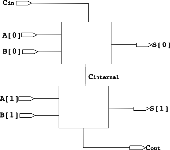
With the full adder we have constructed, we could then use two of these to construct a 2-bit full adder:
module two_bit_full_adder(
       // declare inputs:
       input  Cin,
       input  [1:0] A,
       input  [1:0] B,
       // declare outputs:
       output Cout,
       output [1:0] S);

    // internal carry signal
    wire Cinternal;

    full_adder fa_bit0(Cin,A[0],B[0],Cinternal,S[0]);
    full_adder fa_bit1(Cinternal,A[1],B[1],Cout,S[1]);
endmodule
2
3
4
5
6
7
8
9
10
11
12
13
14
15
Notes:
- In this example A, B and S are all two-bits in size
defined by the slightly strange
syntax
[1:0]. This declares a bit vector with the top index being 1 and the bottom index being 0. It is almost always the case that we use 0 as the bottom index. - Remember that there are two instantiations (i.e. two copies of
the hardware)
of
full_adder, one has the instance namefa_bit0and the otherfa_bit1.
Safety when instantiating modules
The module instantiation we have seen so far uses ordered port connection, which connect a net or variable to a module using the position of the ports of each module definition. This may introduce hard-to-find bugs, e.g.:
module CPU(addr, data, clk, ce, rw);
...
endmodule

module MEM(addr, data, rw, ce, clk);
...
endmodule

wire [15:0] addr;
wire [15:0] data;
wire rw, ce, clk;
//oops, rw connected to clk in CPU module
CPU the_cpu(addr, data, rw, ce, clk);
MEM the_memory(addr, data, rw, ce, clk);
2
3
4
5
6
7
8
9
10
11
12
13
14
If, for example, addr and data were swapped over,
we would end up with a nasty bug but the synthesis tool (i.e. the
compiler for hardware) would produce no error.
There is another style of port connection in Verilog, which is to specify the name of each port explicitly, along with the name of the signal that is connected to that port. For example:
CPU the_cpu(.data(data), .clk(clk), .addr(addr), .rw(rw), .ce(ce));
Using this named port connection style, it is not necessary to maintain the order of the ports for each module instance. The potential for inadvertent design error is reduced, since each port is explicitly connected to a specific net. Also, changing the port ordering in one module does not require change in other modules that instantiate it.
Note: if you don't declare a wire in a module instantiation then SystemVerilog will create a single-bit wire for you, for example:
wire [15:0] addr;
wire rw, ce, clk;
//oops, no data bus declared so it will be just one bit wide
CPU the_cpu(addr, data, rw, ce, clk);
MEM the_memory(addr, data, rw, ce, clk);
2
3
4
5
You pass arguments in the wrong order or the wrong bit-width but no error occurs! Older synthesis and simulation tools provide a warning that is too easy to ignore. While newer tolls (e.g. the verilator simulator you will be using for ticks) is stricter about bit-widths matching, the fact that arguments are usually all collections of bits reduces the effectiveness of type checking.