
Course pages 2015–16
ECAD and Architecture Practical Classes
Yarvi on FPGA
We'll now put the Yarvi on FPGA and integrate it with other peripherals like the screen and rotary encoders. We use Qsys as a rapid way to build up the system-on-chip and plug components together, some from the standard library and others you have built. We could walk you through building the entire system from scratch using the GUI but this is tedious and error-prone, so instead we'll give you a partially built project to speed up the process and reduce possibilities for mistakes.
Download yarvi_fpga.zip and unpack it.
Inside you'll find a number of parts that we'll describe as we go.
As before, yarvi_fpga.qpf is the project file and yarvi_fpga.qsf contains the pin assignments for the DE1-SoC board. We've also added some other files to the project, which are listed in yarvi_fpga.qsf.
Start Quartus and open the yarvi_fpga.qpf Quartus project.
toplevel.sv contains the toplevel Verilog. Open it in Quartus. We've added an instantiation of the Qsys system in there, connecting its ports to FPGA I/O pins like the display, SDRAM and LEDs. We've also wired some pins to static logic levels to turn on the LCD and its backlight.
toplevel.sdc is the timing constraints file, describing the same clocks as before.
We also added yarvi_soc/synthesis/yarvi_soc.qip to the project. This file doesn't exist yet, but yarvi_soc is the name of the Qsys project we will generate and this file instructs Quartus to include the Qsys project that we will make.
Yarvi Qsys system
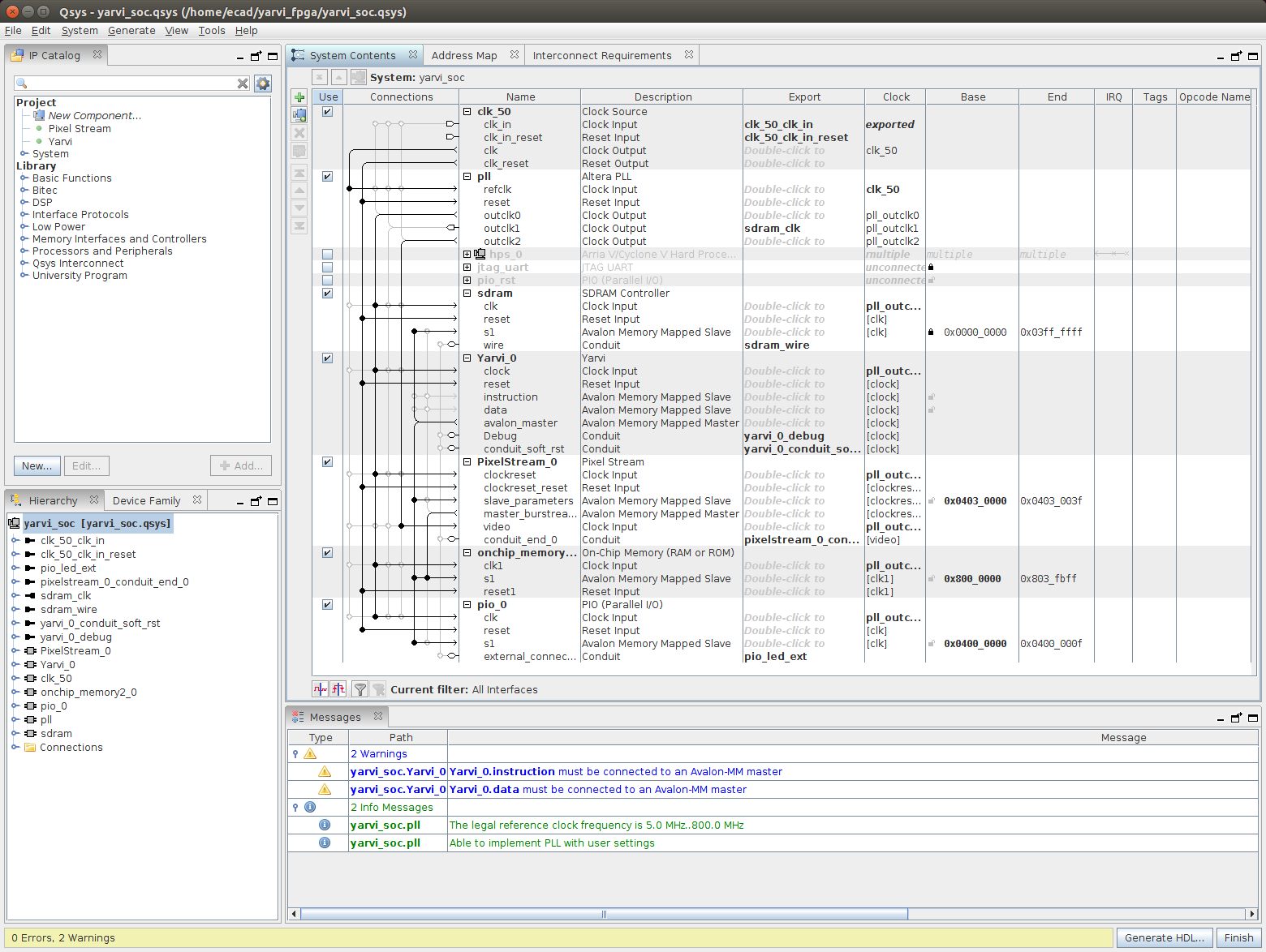
Start Qsys (Tools | Qsys) and open yarvi_soc.qsys. You should see a view similar to the one below.
Erratum: if you get a message Error: yarvi_soc.: list element in braces followed by "}" instead of space go to File | Refresh System or press F5 to rescan the Qsys libraries, and it should now accept it.
We'll first run down the list of components and describe what they are. Many of the peripherals are configurable - double click on the name in bold or right click and Edit... to see what is inside but be sure not to change the settings.

- clk_50: Clock Source
- The clock source accepts a clock and reset from the outside, synchronises the reset to the clock, and then outputs the clock and reset pair as their own clock domain. Qsys keeps track of clock domains and will insert synchronisation for you if you bridge connections from one domain to another. In the toplevel Verilog we have wired the input clock to CLOCK_50, a 50MHz input, and reset to KEY[0], a button on the FPGA side of the DE1-SoC.
- Altera PLL
- A Phase-Locked Loop is an analogue peripheral on the FPGA that is able to generate clocks of different frequencies by multiply and dividing up an input clock. We take in the 50MHz clock and generate three outputs:
Clock name Description outclk0 A 50MHz main clock that is used to clock the rest of the system outclk1 A version of the 50MHz clock with a phase shift of -90 degrees, ie delayed by 5ns. This is exported to the SDRAM chip on the DE1-SoC board. It takes time for the signals to travel from the FPGA across the board and so the clock delay allows the data to become stable before it is latched into the SDRAM chip. outclk2 The 480x272 pixel LCD only supports a limited range of refresh frequencies. We generate a 9MHz pixel clock so that we provide pixels at the appropriate rate to meet the refresh requirements outclk1 is exported to the toplevel as a signal sdram_clk, which is then wired to a pin. The other two clocks we route to other components within Qsys.
- ARM, JTAG UART and pio_rst
There then follow three components which are unticked (disabled) and collapsed. We have left them in the project because their settings are retained so they can easily be re-enabled later. Leave them turned off in this lab.
The Arria V/Cyclone V Hard Processor System is the ARM part of the FPGA. As well as its own DDR3 memory, the ARM part has a number of hard peripherals (like USB controllers, Ethernet, SD card, SPI, etc) that can be enabled in the configuration. Additionally it has a number of bridges that enable the ARM to communicate with peripherals you put in Qsys, like your rotary encoder or you could design a more complex peripheral like a GPU. Each peripheral can appear in the ARM memory map and be accessible from ARM or bare metal code.
The JTAG UART is a simple way to make a text terminal on the FPGA, and we can use it as a terminal from the ARM. We also include a Progammed I/O (PIO) port, that allows the ARM to hold the Yarvi in reset.
- SDRAM controller
- The DE1-SoC includes 64MiB of synchronous DRAM (4Mwords of 16 bits wide). SDRAM requires a certain amount of management (selecting rows and columns, performing refresh of memory cells): the SDRAM controller performs this and translates the native on-FPGA bus into the right format for the SDRAM interface. The interface is exported as wires to the toplevel, where it is connected to the SDRAM chip on the DE1-SoC board.
- Yarvi
We now come to the Yarvi, which we have packaged up in a Qsys form. There are a number of additional interfaces we have exposed to Qsys:
Clock and reset are provided as normal.
The Avalon Memory-Mapped Master is the Yarvi's main memory interface, where it can access all peripherals and memory except the 4KiB of instruction memory and 4KiB of data memory it has inside. See how the avalon_master port on Yarvi is connected to Avalon Memory Mapped Slave ports on other devices like the SDRAM, on-chip memory and PIO. This means all these devices become accessible from Yarvi load and store instructions.
instruction and data are Avalon Memory-Mapped Slave ports, which allow the ARM (or another Yarvi) to read and write the Yarvi's internal memories. This gets around the problem in Tick 1 which prevented loading code on the Yarvi, and allows programs and data to be loaded and stored. In a single Yarvi system we aren't using them, so they are unconnected (you can safely ignore the warning that they must be connected to an Avalon-MM Master).
Debug and conduit_soft_rst allow another processor to pause and reset the Yarvi, for instance during and after loading code. We simply export them and wire them inactive in the top level.
- PixelStream and video_memory
- Video formats originate from the cathode ray tube, where electron beam(s) scan the pixels on the screen left to right, top to bottom. The electromagnets directing the e-beam have inertia, which means that the beam cannot pause or go back: when the beam passes a pixel, it lights it with whatever colour is presented to it that moment. The result is that scanning is a hard timing deadline: you cannot be late with a pixel.
To drive the display, we need two functions. First, we need some memory to hold the pixel data we want to display. For 480 horizontal by 272 vertical pixels at 16 bits per pixel, that requires 480*272*2 = 261120 bytes. Then we need a device to generate the timing of the display - in this case a line (horizontal) rate of 17.142kHz and a frame (vertical) rate of 59.5Hz. For each pixel we must read the data out of memory and have it ready to present within a short time window.
To meet the timing deadlines and not have to fight for bandwidth for the slow SDRAM, we have added an On-Chip Memory to act as Video RAM. The Cyclone V FPGA in the DE1-SoC has about 4Mbit of block RAM which can be used by FPGA logic, or the On-Chip Memory component allows us to use it as RAM or ROM - here we configure about 2Mbit as a 32 bit wide RAM.
PixelStream acts as the display controller, performing memory (DMA) reads from the video RAM and driving the display timing. PixelStream was actually written in Bluespec SystemVerilog, a higher-level hardware defintion language derived from Haskell that compiles to Verilog (the source is included in the PixelStream folder)
- pio_0
A PIO, or Programmed I/O, is a simple interface that turns memory writes into outputs, or memory reads into inputs. We have added a 10-bit output PIO which is connected in the toplevel to the row of red LEDs.
Yarvi memory map
Click on the avalon_master line in Yarvi_0. This highlights the devices connected to the Yarvi memory master, that Yarvi can initiate reads from and writes to. Look in the Base and End columns. Each device fits in a block of memory, the size depending on its function. You can set the Base to decide at what address it begins. For instance the pio_0 lives between 0x04000000 and 0x0400000f inclusive (ie is 16 bytes or 4x 32-bit words long).
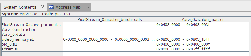
You'll see this more clearly in the Address Map tab (use the View menu if it is hidden). We have multiple memory masters on the FPGA, and each can have a different memory map, either sharing or not sharing peripherals. Each column in the Address Map view is a different master. For instance, on this view we can see that the video_memory can be accessed by both the Yarvi and the PixelStream. It so happens that in both memory spaces it is set to start at 0x08000000, but it need not be the case. (PixelStream has a 64 bit address port and Yarvi a 32 bit address port, which is why the PixelStream is prefixed with more zeroes)
Yet another perspective on memory can be seen inside Yarvi itself. Yarvi has its own internal data memory that Qsys does not know about. To avoid clashes, we remap the Qsys address space. The Yarvi_0.avalon_master memory (from 0 to 0x0803fbff) is fitted into Yarvi address space in the range 0x80000000 to 0x8803fbff. In other words, in Yarvi's 4GiB address map, the lower 2GiB is used for Yarvi internal memory/peripherals and the upper half for memory and peripherals we define in Qsys.
You can change the base addresses by clicking on them, either in the System Contents or Address Map views. If you aren't fussy about your memory layout Qsys can also assign addresses for you (System | Assign Base Addresses) - some of them are locked to prevent Qsys changing them by accident.
We'll add some more components to the Qsys system later, but for the moment just Generate your Qsys system. You can carry on reading while it generates.
Yarvi sofware in FPGA
Next, have a look in the yarvi_fpga/yarvi folder. The Yarvi itself is mostly unchanged from the simulation version. All we have done is added a directive to tell Quartus to implement the memories containing the instruction and data memories as Memory Initialisation Files (MIF files), which means we can set the contents when we build the FPGA. This is simply a different format from the .txt that we used in simulation.
Go into yarvi_fpga/yarvi/software. This should also look familiar, but we have changed the Makefile to generate MIF files for Quartus (the names are specified in the Qsys settings on the Yarvi component). We have also changed the avalon_addr.h to move the framebuffer into video RAM from SDRAM as we used in the emulator.
Open main.c. This is a simple program to count on the LEDs. Notice that we use avalon_addr.h to define the memory locations we set in Qsys: there is no automatic mapping, so if you change an address in Qsys you need to amend the header file to match.
Change to this directory in your terminal and type make. You should see some .mif files appear in yarvi_fpga/yarvi/. You have now built the software for your Yarvi.
Building the FPGA
Now is the time to build the template FPGA and check that your Yarvi is indeed counting on the LEDs. Making sure that you have generated your Qsys and built your software, you can now start a Quartus build. This build may take 15 minutes or so - if you are able to give more RAM or more CPUs to your VM it will likely improve compile times (but you'll have to shut down the VM to change those settings in VirtualBox).
Once built, download your project to your FPGA and check that the LEDs are counting. If so, you are successfully executing code.
Updating your software
We don't want to have to resynthesise the FPGA each time we change the software, and Quartus provides us with a shortcut. Change your software in some way - for instance make it count down instead of counting up. Rebuild the software. Then go back to Quartus and go to Processing | Update Memory Initialisation File. Wait for this to complete, then run Processing | Start | Start Assembler. The Assembler is the last stage of FPGA compilation that generates the bitfile that is downloaded to the FPGA, and allows updating the memory contents without redoing the place and route.
Erratum: we had the buttons order in the display emulator reversed compared with the hardware. The correct order, which has been updated in the yarvi_fpga/yarvi/software/avalon_addr.h file and on the shift register exercise is as follows. You may wish to amend your button reading code as appropriate.
Note that, because the spare pins, temperature and touch signals may be either 0 or 1, you need to mask off the bits (AND them with a bitmask) to isolate the specific bit you want – it is not enough simple to read the shift register and check if it is non-zero to detect if buttons are pressed.
| Input | Bit |
|---|---|
| BUTTON_B | 15 |
| BUTTON_A | 14 |
| BUTTON_Y | 13 |
| BUTTON_X | 12 |
| SPARE_IN_0 | 11 |
| TOUCH_IRQ | 10 |
| SPARE_IN_1 | 9 |
| SPARE_IN_2 | 8 |
| NAV_U | 7 |
| NAV_L | 6 |
| NAV_R | 5 |
| NAV_D | 4 |
| NAV_CLICK | 3 |
| DIALR_CLICK | 2 |
| DIALL_CLICK | 1 |
| TEMPERATURE_ALARM | 0 |
You can now download the bitfile to your board again and check the software has been updated.
Because this is something you might do regularly, we have added the commands to the software Makefile. Running make updatemif will build your software and then update the bitfile ready to download. We have also added make download to automate that part as well if you wish.