
Course pages 2015–16
ECAD and Architecture Practical Classes
Development workflow
A typical work-flow for FPGA design may be separated into three main stages:
- Architecture
- Describing your design at various levels of abstraction. The most basic components, from synchronisers to simple processors, are written in an HDL, such as SystemVerilog; these are then combined (recursively) to form more complex systems.
- Simulation and Synthesis
- Simulation tests your design by emulating hardware matching the semantics of the HDL. Synthesis is the compilation of your design into a netlist, expressing it in terms of FPGA elements (e.g. wiring, LUTs, etc.).
- Software
- Processor architectures can run programs compiled to the appropriate binary (machine code) format. A binary is executed by reading its instructions from the device memory; some binaries may be incorporated into the device programming file, others uploaded dynamically.
A general overview is given by the following schematic; the labs provide greater coverage.
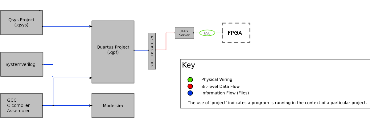
- Yarvi
- A processor written in SystemVerilog that implements the RISC-V instruction set.
- GCC
- C compiler and assembler produces binaries (machine code) for the RISC-V processor. Source code edited with your favourite editor.
- Modelsim
- Provides a simulation environment for (System)Verilog, enables fine-grained debugging of hardware components.
- Quartus
- Hardware IDE. Using an HDL, such as SystemVerilog, a Quartus project is a hierarchy of components or modules from a specified root. A complete project may be synthesised for programming onto a specified FPGA device.
- Qsys
- Qsys works at the component level of abstraction. A component in Qsys is a black box with a specified interface (wires), which can be connected together using a switched interconnect memory system. Each black box is ultimately a set of files in some HDL. Each Qsys project thus represents a hierarchy of Verilog components (much like a Quartus project), meaning it can also be treated as a component for use in another project.
- Programmer / DE1-SoC
- JTAG is a communication protocol for on-chip debug (e.g. via a JTAG UART) and programming, using a standard group of dedicated pins. The FPGA is primarily configurable as a switch fabric and lookup tables, the former controlling connections between wires and the latter implementing custom functions. The control logic of each configurable element is memory-mapped to a dedicated SRAM module. An SRAM Object File (.sof), produced by a Quartus compilation, contains configuration data for each element, which is loaded via JTAG into the corresponding (volatile) SRAM module to (temporarily) program the FPGA.
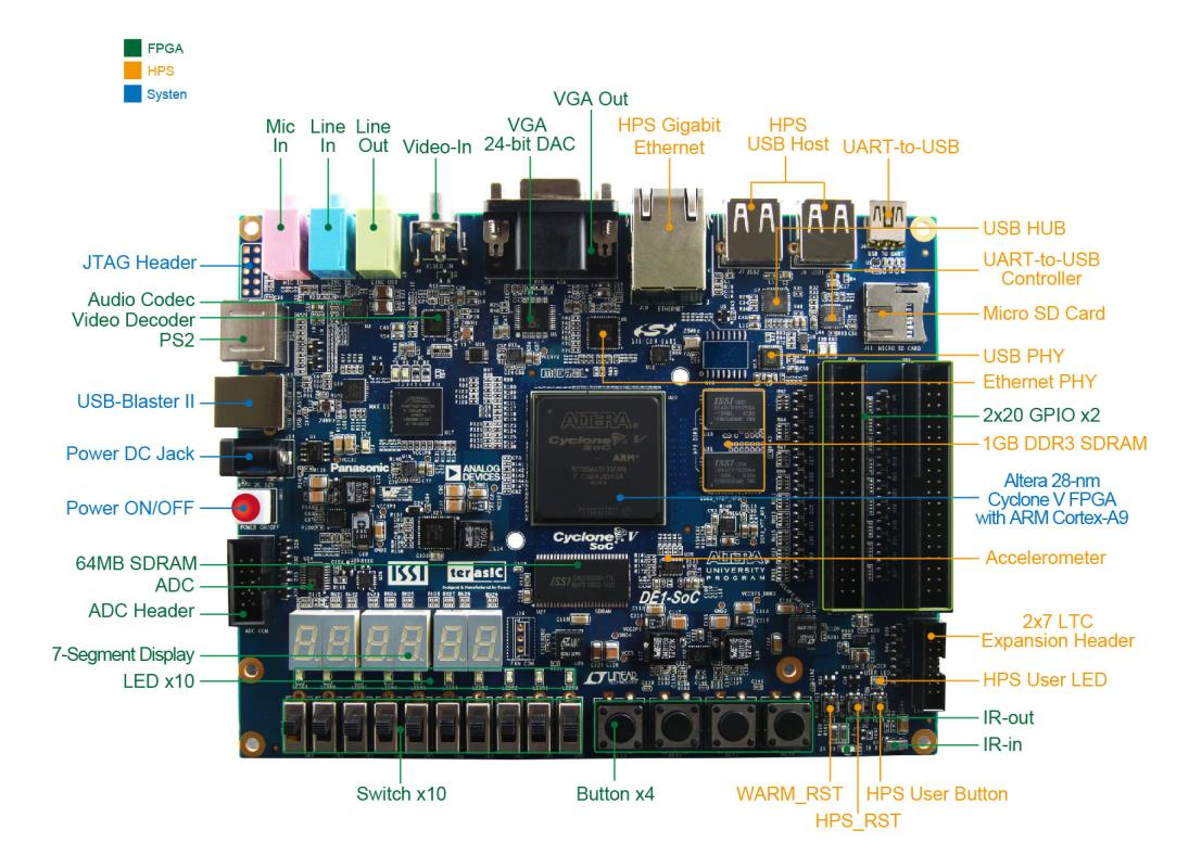
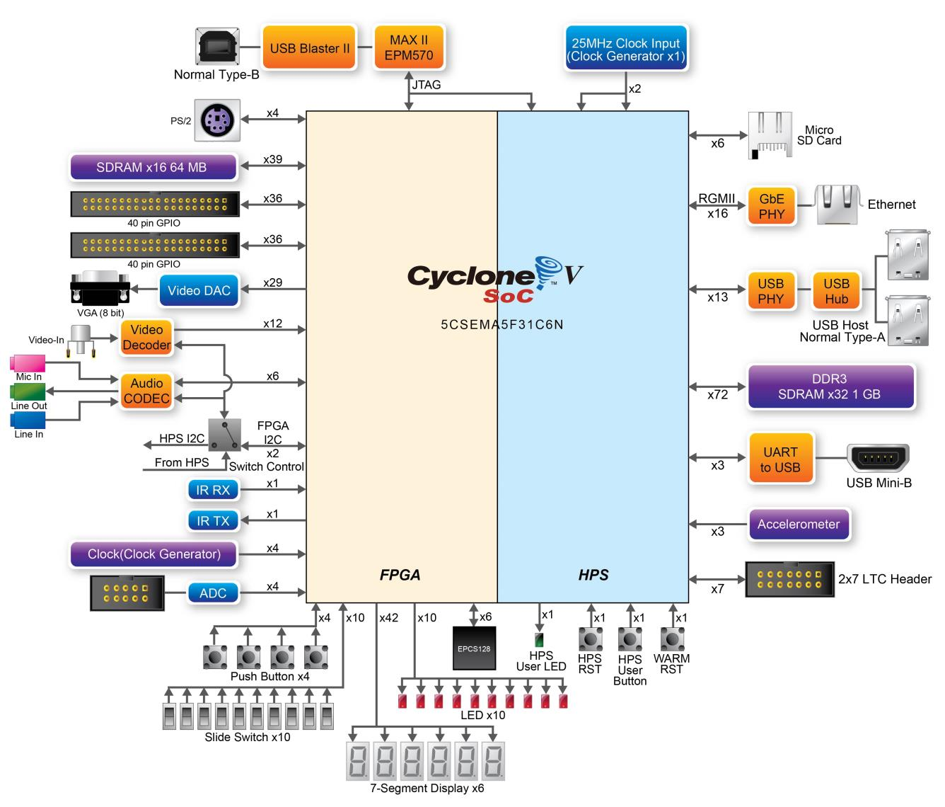
The DE1-SoC FPGA board
In this lab we'll be using the DE1-SoC FPGA board from Terasic. The board contains a medium-sized Altera Cyclone V SoC FPGA, which is composed of two parts: the FPGA logic that you will be programming in this lab, and a dual-core Cortex A9 ARM processor (the `Hard Processor System' or HPS), which is able to run Linux or FreeBSD and tightly couple with peripherals you design on the FPGA. Each side has a number of I/O ports connected to it, that can be driven from either FPGA or ARM – for instance there is separate RAM for ARM and FPGA. We won't use the ARM side in this lab, but it is available for projects and further exploration.
Cambridge add-on board
To complement the DE1-SoC we have designed our own board to provide a display and more inputs. You will write code to drive some of the peripherals during the lab.
