
Course pages 2017–18
ECAD and Architecture Practical Classes
Development workflow
A typical work-flow for FPGA design may be separated into three main stages:
- Architecture
- Describing your design at various levels of abstraction. The most basic components, from synchronisers to simple processors, are written in a HDL, such as SystemVerilog; these are then combined (recursively) to form more complex systems.
- Simulation and Synthesis
- Simulation tests your design by emulating hardware matching the semantics of the HDL. Synthesis is the compilation of your design into a netlist, expressing it in terms of FPGA elements (e.g. wiring, LUTs, etc.).
- Software
- Processor architectures can run programs compiled to the appropriate binary (machine code) format. A binary is executed by reading its instructions from the device memory; some binaries may be incorporated into the device programming file, others uploaded dynamically.
A general overview is given by the following schematic; the labs provide greater coverage.
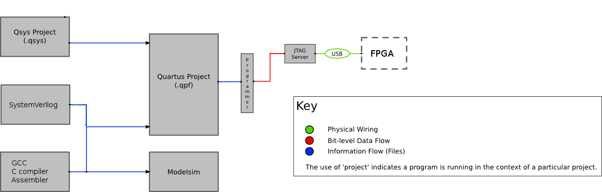
- Clarvi
- A processor written in SystemVerilog that implements the RISC-V instruction set.
- GCC
- C compiler and assembler produces binaries (machine code) for the RISC-V processor. Source code edited with your favourite editor.
- Modelsim
- Provides a simulation environment for (System)Verilog, enables fine-grained debugging of hardware components.
- Quartus
- Hardware IDE. Using an HDL, such as SystemVerilog, a Quartus project is a hierarchy of components or modules from a specified root. A complete project may be synthesised for programming onto a specified FPGA device.
- Qsys
- Qsys works at the component level of abstraction. A component in Qsys is a black box with a specified interface (wires), which can be connected together using a switched interconnect memory system. Each black box is ultimately a set of files in some HDL. Each Qsys project thus represents a hierarchy of Verilog components (much like a Quartus project), meaning it can also be treated as a component for use in another project.
- Programmer / DE1-SoC
- JTAG is a communication protocol for on-chip debug (e.g. via a JTAG UART) and programming, using a standard group of dedicated pins. The FPGA is primarily configurable as a switch fabric and lookup tables, the former controlling connections between wires and the latter implementing custom functions. The control logic of each configurable element is memory-mapped to a dedicated SRAM module. An SRAM Object File (.sof), produced by a Quartus compilation, contains configuration data for each element, which is loaded via JTAG into the corresponding (volatile) SRAM module to (temporarily) program the FPGA.
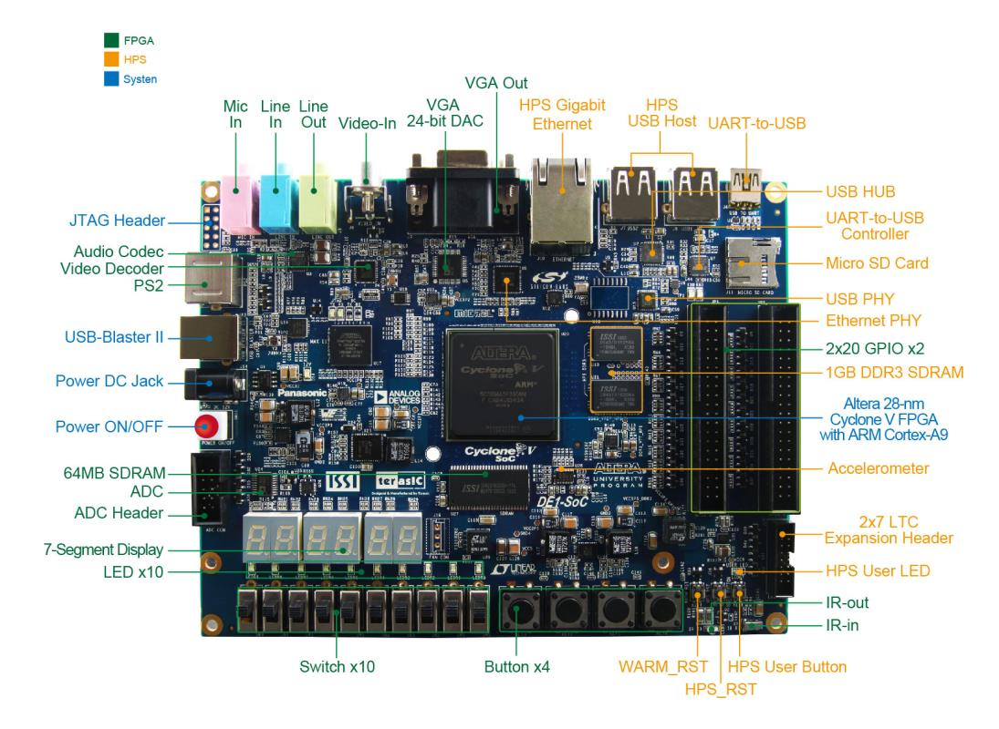
The DE1-SoC FPGA board
In this lab we'll be using the DE1-SoC FPGA board from Terasic. The board contains a medium-sized Altera Cyclone V SoC FPGA, which is composed of two parts: the FPGA logic that you will be programming in this lab, and a dual-core Cortex A9 ARM processor (the `Hard Processor System' or HPS), which is able to run Linux or FreeBSD and tightly couple with peripherals you design on the FPGA. Each side has a number of I/O ports connected to it, that can be driven from either FPGA or ARM – for instance there is separate RAM for ARM and FPGA. We won't use the ARM side in this lab due to complexity and long synthesis times, but it is available for projects and further exploration.

Cambridge add-on board
To complement the DE1-SoC we have designed our own board to provide a display and more inputs. You will write code to drive some of the peripherals during the lab.
