Course pages 2017–18
ECAD and Architecture Practical Classes
Introduction to FPGA synthesis
Synthesis is the process of mapping Hardware Description Language (HDL) code, such SystemVerilog, on to the basic units provided by a FPGA e.g. LUTs, wiring, memory etc. You will use the Quartus synthesis tool in these labs. This part of the lab guides you through creating a Quartus project, synthesising HDL and programming and testing it on the FPGA.
Hardware
Ask a demonstrator to sign you out an FPGA board.
Creating a Quartus Project
First, create a directory called exercise2 and then create a new directory for this project inside, perhaps called ecad_fpga_1.
Important: Some tools in Quartus do not like paths with spaces in, so ensure all file and directory names you choose do not have spaces in them.
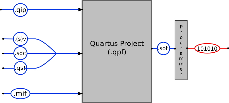
Download the following files into the new directory:
- toplevel.sv
- Top-level SystemVerilog file. Quartus projects use multiple SystemVerilog modules to implement a complete FPGA design. The top-level file contains the module which instantiates all of the other modules and which is used to connect them to the FPGA's pins.
- toplevel.sdc
- A design constraints file. Describes the hardware clocks that are connected to the FPGA. Quartus uses information about the clocks to decide if a synthesised design will run correctly or experience timing issues.
- de1soc_pin_assignments.qsf
- Pin assignments file. To interact with the hardware, this file matches (groups of) pins (e.g. those for the red LEDs) on the device to 'friendly' names (e.g. so the red LEDs can be named LEDR[9:0]) in the top-level SystemVerilog file.
Start Quartus
Start Quartus by opening a new terminal (and running your setup script if on MCS). Type:
quartus &
Quartus may report it cannot connect to the license server - this is not a problem for these labs. Please ignore any Quartus upgrade messages since we wish to stick with the version we have for the duration of the labs.
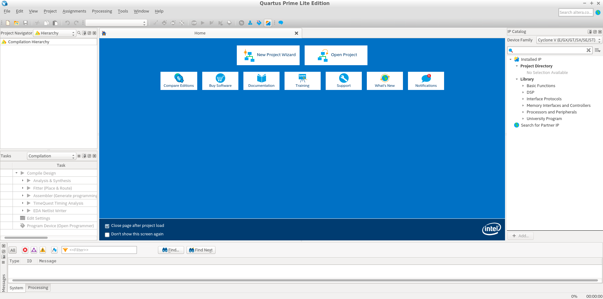
Once Quartus has started, it should resemble the screenshot to the right. At the bottom is the Messages pane, which displays compilation messages and warnings; this may be useful when trying to debug your project. On the left is the Project Navigator, the first tab shows the logical hierarchy of the project. Below this the Tasks pane shows the state of compilation.
Create a New Project
Select File | New Project Wizard and click Next to display the screen where you can set the name and working directory for the project. In the top box, enter the directory where you downloaded the 3 files above. In the second box, enter a name of the project; this can be whatever you like, though we recommend ecad_fpga. In the bottom box, type toplevel since this is the name of the top-level SystemVerilog module for this project. Now click Next.
Say you want to make an Empty project and click Next.
On the next page, click Add All to add the SystemVerilog and SDC files you downloaded earlier into the project. If these files do not appear in the list, ensure you have saved them in the same directory that you specified as the working directory in the previous step. Now click Next.
This page lets you select the type of FPGA used by the project. In the drop down boxes at the top, select family Cyclone V (E/GX/GT/SX/SE/ST), device Cyclone V SE Mainstream, package FBGA, pin count 896 and speed grade 6 and ensure that Specific device selected in 'Available devices' list is selected. Next, in the Available devices list at the bottom, select 5CSEMA5F31C6. This is the part number of FPGA that is on the DE1-SoC board. Check the device you have selected has 32070 ALMs to confirm before clicking Next.
In EDA Tool Settings, make sure all the Tool Names and Formats you can change are set to None. This prevents Quartus depending on additional third-party tools.
Now click Finish to complete project setup.
Import Pin Assignments
You need to import the pin assignments from the .qsf file you downloaded earlier. To do this, select Assignments | Import Assignments... click on the button labelled "..." and select the de1soc_pin_assignments.qsf file. Click OK to import the assignments.
Important: Failure to import pin assignments will result in your design not being connected to the outside world. Quartus will optimise it to nothing since it doesn't have any used input and output signals. You must import the pin assignments in every project you create, including new projects. Just copying the .qsf file isn't enough.
Select HDL
Quartus uses Verilog 2001 as the default HDL but we'll be using SystemVerilog throughout. Select Assignments | Settings... and then click on Compiler Settings | Verilog HDL Input in the window that opens and then select SystemVerilog. Then click Apply and OK.
Save these changes by selecting File | Save Project.
Example code
As supplied, the top level template doesn't do anything. Open the toplevel.sv in Quartus: To open up toplevel.sv, look in the Project Navigator pane, select the Files tab and double click on toplevel.sv. You may need to open up Quartus full screen to see the panes more clearly.
Add some code to the toplevel module to count on the row of red LEDs:
    logic [27:0] count;

    always_ff @(posedge CLOCK_50) begin
        count <= count + 1;
    end

    always_comb begin
        LEDR <= count[27:18];
    end
CLOCK_50 and LEDR are external signals provided to the FPGA that get routed into these signals in your SystemVerilog.
Synthesis
You should now be able to compile the project and use it to program the DE1-SoC.
Compilation
Select Processing | Start Compilation to compile the project (alternatively, press Ctrl + L or press the Play button on the button bar). If asked to save toplevel.sv before continuing, click Yes. During compilation it is almost certain that warnings will appear in the messages pane at the bottom of the screen. You should always read these through carefully since they can sometimes help you find bugs in your project much faster than waiting for them to manifest. However, due to the unfortunate design of the tools, most of the warnings will be of no consequence and can be safely ignored. In particular, many more warnings are generated if you forgot to import the pin assignments. If there are any errors about licensing, call a demonstrator for help.
There are four different kinds of messages output, which can be hidden and revealed with buttons at the top of the messages window:
- Errors
- Red, cause your compilation to halt and must be fixed to proceed
- Critical warnings
- Purple, problems which don't stop the compilation from proceeding but is highly recommended that you pay attention. In many cases the system won't work with critical warnings.
- Warnings
- Blue, you can skim through but most of them are informational and don't need attention. If you have a problem, however, it is worth looking through these messages to see if they mention anything of relevance.
- Information
- Green, information about the progress of compilation.
When you compile you should check for errors and critical warnings.
Timing Analysis
A hardware clock is a signal (square wave) generated by an analogue oscillator. Quartus can infer which wires in your design, such as CLOCK_50, will carry a clock signal based on how they are used in the HDL. Each combinational path between two registers has a maximum update latency; for each clock wire, the longest combinational path between the registers it controls dictates the maximum frequency of the oscillator that may be used to drive it. If an oscillator has a higher frequency than this, it is said that the design "does not meet timing" and it is unlikely to work.
Select the Compilation Report tab and expand TimeQuest Timing Analyzer. Expand the Slow 1100mV 85C and Slow 1100mV 0C models and check the Fmax Summary; frequencies above 50MHz indicate it is safe to use the 50MHz oscillator on the board, as defined in the pin assignments you imported. Each model accounts for different latencies due to operating temperature (0C/85C) and manufacturing variations (Slow/Fast).
Timing analysis is made accurate by specifying the clocks used via a Synopsys Design Constraints file (such as toplevel.sdc) to describe the oscillator(s) driving the wires used as clocks in your design. This allows Quartus to generate a critical warning if an oscillator frequency exceeds the corresponding Fmax. Note that Quartus will still finish compilation and allow you to program the FPGA even if a design fails to meet timing. If a design doesn't work on the FPGA, check if there are any timing warnings, as well as other warnings that could indicate HDL bugs.
Programming
Next, ensure your DE1-SoC is connected to the power supply and that the power supply is plugged into a mains socket and turn it on. The blue LED next to the power socket should turn on and some other LEDs may come on or flash. The backlight on the LCD should also come on. If not call a demonstrator for help.
Using the full-size USB-B socket labelled USB BLASTER (nearest to the power socket), connect the DE1-SoC to your computer.
As a simple test that the board is plugged in and communicating, go to a terminal (sourcing the setup script on the MCS) and type:
jtagconfig
The first time after board powerup some USB firmware is downloaded to the board, then it changes its USB ID and reconnects. It may not be fast enough to detect the board first time if you are in a VM. Try two or three times if you get 'programming cable not detected'. You are aiming for output similar to:
1) DE-SoC [3-2]
  4BA00477   SOCVHPS
  02D120DD   5CSE(BA5|MA5)/5CSTFD5D5/..
This shows that two devices on the JTAG chain have been detected: no. 1 is the HPS (ARM core), and no. 2 is the 5CSEMA5 FPGA device. If you successfully receive this output your FPGA is communicating with your PC. If you power off your board you may have to run jtagconfig again to re-establish communications. (lsusb will tell you if an Altera device is visible to your VM - if nothing appears you likely have a VM problem. Make sure you have followed the USB setup instructions in the Pre-lab Setup section)
In Quartus, select Tools | Programmer, and at the top make sure DE-SoC ... appears next to Hardware Setup.... If not, click on Hardware Setup..., double click DE-SoC in the list box and then click Close. If the DE-SoC does not appear, call a demonstrator for help.
Click Auto Detect. If you are asked to select a device, pick 5CSEMA5. You should see a picture of the two devices on the JTAG chain, and two lines that relate to them.
Double click <none> next to 5CSEMA5 and select the file called toplevel.sof that is probably in output_files in your project folder. This is the file that was compiled by Quartus and that we are going to use to program the FPGA. Tick Program/Configure. Click Start to program the FPGA. After a few seconds you should see the LEDs on the board flashing. If this doesn't happen, check the warnings that Quartus produced during compilation. If the seven-segment displays are displaying an odd pattern this means that you forgot to import the pin assignments.
Optional: explore your synthesised design
Quartus takes your HDL and maps it onto logic blocks that exist on the FPGA, and it provides visualisation tools to see what it did. In normal development we tend not to use them much, but can be useful if you want to see how the process works or perhaps if you want to see how it handled a particular piece of HDL code. Some of these will require much scrolling or a large monitor!
Now you have synthesised a counter, have an explore of various menu options:
- Tools | Netlist viewers | RTL viewer
- This shows you the logic schematic that your RTL made, before much transformation was done on it. It shows the hierarchies of modules and system operators, and how they are wired together.
- Tools | Netlist viewers | Technology map viewer
- Here you can follow the various transformations the logic underwent. For example the counter is expanded into a series of flip-flops, with combinational logic to calculate the next state. Notice how carries are used to pass logic from one cell to the next. This view shows it in a format that uses the underlying logic primitives present on the Cyclone V. (Note there can be multiple pages displayed, so you may need to use the page selector at the top right)
- Tools | Netlist viewers | State machine viewer
- Quartus can refactor state machines to make them more efficient. This shows what it did.
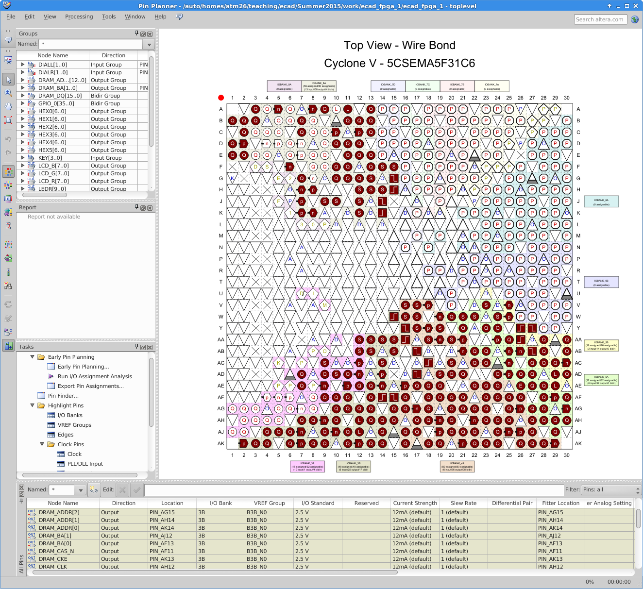
- Assignments | Pin Planner
- This enables you see how all the pins on the FPGA are mapped to the physical package. Pins are grouped in banks (different colours) which share particular properties such as proximity and voltage settings, for example all the DRAM_ pins on the DE1-SoC are mapped to bank 3B, which is the lower middle of the chip as it is displayed. (click to enlarge)
- Tools | Chip Planner
- This shows you a top level overview of the chip, as routed.
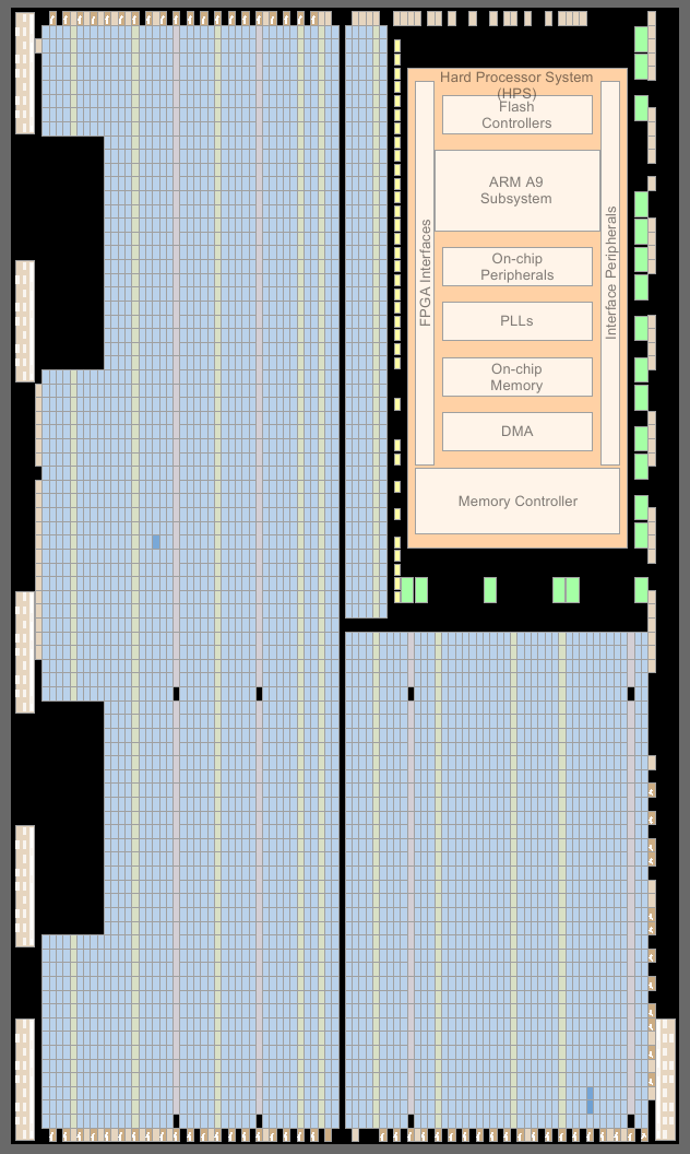
Pins are arranged around the edge, with larger PLL blocks. At the top right is the Hard Processor System block containing the ARM, its memory controller and peripherals. There are also configurable hard peripheral blocks in green, for example Ethernet MACs.
In the rest of the chip is a sea of logic (LAB) blocks. Arranged in columns can be seen coarse grained memory blocks (M10K, having 10Kbits) and DSP blocks (fast multiply and other arithmetic).
Click around to identify some of the blocks - look in the Resource properties box for details on each one.
Some of the blocks are darker coloured, which means they have non-zero logic utilization. Select a block, zoom in (a lot) and you'll see the sub-blocks within them. Zoom in more and you'll see sub-sub-blocks like LUTs and flip-flops. Select one, right click and go to Locate Node -> Locate in Resource Property Editor. This should show you a diagram of the element, for example a LUT with placement of the connections and the contents of the lookup tables.
For example, this is the placement for bits 0 and 1 of the counter we just made (click to enlarge):
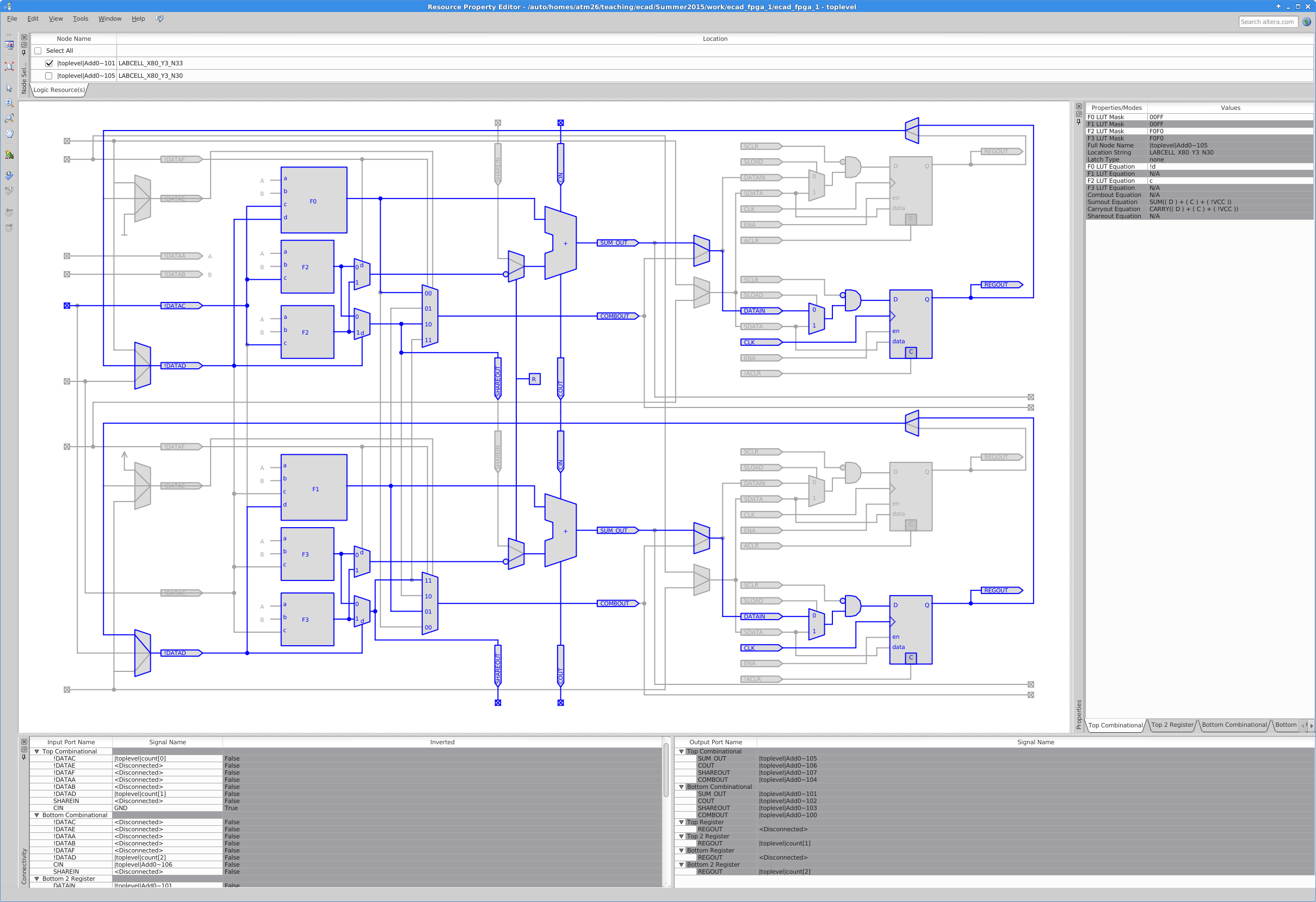
The grey lines are the hard structure of the block, and the blue lines are the connections Quartus made for us using them. Notice how the inputs are routed into the LUTs, the adder and then the flip-flops. Also notice the fast carry chain connecting the blocks vertically.