
Course pages 2017–18
ECAD and Architecture Practical Classes
Exercise 5: Clarvi on FPGA
We'll now put the Clarvi on FPGA and integrate it with other peripherals like the screen and rotary encoders. We use Qsys as a rapid way to build up the system-on-chip and plug components together, some from the standard library and others you have built. We could walk you through building the entire system from scratch using the GUI but this is tedious and error-prone, so instead we'll give you a partially built project to speed up the process and reduce possibilities for mistakes.
Make a new directory exercise5. Download clarvi_fpga.zip and unpack it inside (so you have exercise5/clarvi_fpga).
Inside you'll find a number of parts that we'll describe as we go.
As before, clarvi_fpga.qpf is the project file and clarvi_fpga.qsf contains the pin assignments for the DE1-SoC board. We've also added some other files to the project, which are listed in clarvi_fpga.qsf.
Start Quartus and open the clarvi_fpga.qpf Quartus project.
clarvi_fpga.sv contains the toplevel Verilog. Open it in Quartus. We've added an instantiation of the Qsys system in there, connecting its ports to FPGA I/O pins like the display and LEDs. We've also wired some pins to static logic levels to turn on the LCD and its backlight.
toplevel.sdc is the timing constraints file, describing the same clocks as before.
We also added clarvi_soc/synthesis/clarvi_soc.qip to the project. This file doesn't exist yet, but clarvi_soc is the name of the Qsys project we will generate and this file instructs Quartus to include the Qsys project that we will make.
Clarvi Qsys system
Start Qsys (Tools | Qsys) and open clarvi_soc.qsys. You should see a view similar to the one below.

We'll first run down the list of components and describe what they are. Many of the peripherals are configurable - double click on the name in bold or right click and Edit... to see what is inside but be sure not to change the settings.

- clk_50: Clock Source
- The clock source accepts a clock and reset from the outside, synchronises the reset to the clock, and then outputs the clock and reset pair as their own clock domain. Qsys keeps track of clock domains and will insert synchronisation for you if you bridge connections from one domain to another. In the toplevel Verilog we have wired the input clock to CLOCK_50, a 50MHz input, and reset to KEY[0], a button on the FPGA side of the DE1-SoC.
- Altera PLL
- A Phase-Locked Loop is an analogue peripheral on the FPGA that is able to generate clocks of different frequencies by multiply and dividing up an input clock. We take in the 50MHz clock and generate two outputs:
Clock name Description outclk0 A 50MHz main clock that is used to clock the rest of the system outclk1 The 480x272 pixel LCD only supports a limited range of refresh frequencies. We generate a 9MHz pixel clock so that we provide pixels at the appropriate rate to meet the refresh requirements - PixelStream and video_memory
-
Video formats originate from the cathode ray tube, where electron beam(s) scan the pixels on the screen left to right, top to bottom. The electromagnets directing the e-beam have inertia, which means that the beam cannot pause or go back: when the beam passes a pixel, it lights it with whatever colour is presented to it that moment. The result is that scanning is a hard timing deadline: you cannot be late with a pixel.
To drive the display, we need two functions. First, we need some memory to hold the pixel data we want to display. For 480 horizontal by 272 vertical pixels at 16 bits per pixel, that requires 480*272*2 = 261120 bytes. Then we need a device to generate the timing of the display - in this case a line (horizontal) rate of 17.142kHz and a frame (vertical) rate of 59.5Hz. For each pixel we must read the data out of memory and have it ready to present within a short time window.
To meet the timing deadlines and not have to fight for bandwidth for the slow SDRAM, we have added an On-Chip Memory to act as Video RAM. The Cyclone V FPGA in the DE1-SoC has about 4Mbit of block RAM which can be used by FPGA logic, or the On-Chip Memory component allows us to use it as RAM or ROM - here we configure about 2Mbit as a 32 bit wide RAM.
PixelStream acts as the display controller, performing memory (DMA) reads from the video RAM and driving the display timing. PixelStream was actually written in Bluespec SystemVerilog, a higher-level hardware definition language derived from Haskell that compiles to Verilog (the source is included in the PixelStream folder)
Adding a Clarvi
At present, the system simply displays the contents of the video memory on the screen, and that's it. Let's add some more components.
From the IP Catalog side panel, double-click on Clarvi. A dialogue will pop up asking about memory widths and initial addresses for program counter and trap vector. Set the DATA_ADDR_WIDTH to 29 bits, leave the rest unchanged and click Finish. You'll see an empty Clarvi appear in your system.
Next add an On-Chip Memory (RAM or ROM) (in Basic Functions->On Chip Memory in IP Catalog). You want a RAM, 32 bits wide, size 65536 bytes, with a non-default initialization file of mem.hex. (Recall mem.hex is output by the Clarvi software Makefile). Because Clarvi can issue two memory operations per cycle (one instruction read and one data load/store) it needs dual-port access. Finish to create the memory for Clarvi's program and data.
Now you'll need to connect them up as follows:
- For each, wire up the reset to the reset output of clk_50. Wire up clock to the outclk0 of the PLL. Clarvi will thus run off a 50MHz clock generated by the PLL, which we can adjust speed later if we wish. For the On-Chip Memory each memory port has a separate clock and reset - connect both of these up.
- Next, Clarvi has two memory ports, one for instruction and a 'main' port for data. Wire main to the on-chip memory slave s1, and instr to on-chip memory slave s2. Likewise wire just main to the video memory slave s1.
- Also wire main to PixelStream's slave_parameters port (this allows us to reconfigure the display size). Don't worry if you get a warning about address overlaps at this stage.
- You can leave Clarvi's interrupt_receiver and debug ports unconnected (ignore Qsys' warning).
Clarvi inputs and outputs
Now we want to interface Clarvi to our other hardware, which we'll do via Parallel I/O (PIO) components. These are simple memory-mapped components that allow the CPU to read or set external wires that can be connected to outside inputs and outputs.
Find the PIO in the IP Catalog. We want to add 5 PIOs:
- 10 bits output for the LEDs
- 24 bits output for the hex digits
- 8 bits input for the left dial
- 8 bits input for the right dial
- 16 bits input for the display buttons
(If you did the Optional exercise you can also add some extra PIO outputs for volume, note and octave.)
By default they're given unhelpful names like pio_5. To distinguish them, right click the top line of each one, select Rename and give them a meaningful name.
Connect up the clk, reset, and s1 memory-mapped slave ports to the same clock, reset and 'main' memory master as Clarvi. Double click the external_connection entry in the export column to export a bundle of wires to wire the inputs/outputs.
Now we need to configure the memory map, where each device can be accessed from software, because likely they're all on top of each other and Qsys is complaining. You can do this with the Base column of the System Contents tab, but you may find it easier to use the Address Map tab (use the View menu if it is hidden).
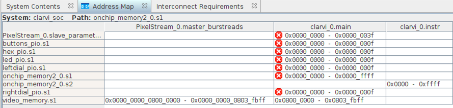
Inside our system-on-chip, we have a number of memory-mapped masters, who are able to initiate memory reads and writes, and some memory-mapped slaves, who 'consume' and reply to those requests. Qsys displays the masters as columns and the slaves as rows.
This table sets out the address ranges that, for a given master, a particular slave will be selected to respond. In our system we see Clarvi's two instruction and data masters, and an additional master for PixelStream to fetch pixels from video memory when it sends them to the screen. Each master can have a different address map, that is a different view of which slaves respond at which addresses.
We'll configure our components to match the address map we used in the Clarvi simulator:
| Component | Clarvi data master base (clarvi_0.main) | Clarvi instruction master base (clarvi_0.instr) |
|---|---|---|
| PixelStream parameters | 0x04001000 | |
| Video memory | 0x08000000 | |
| Data memory (onchip_memory2_0.s1) | 0x0 | |
| Instruction memory (onchip_memory2_0.s2) | 0x0 | |
| LED PIO | 0x04000000 | |
| Hex digits PIO | 0x04000080 | |
| Left dial PIO | 0x04000100 | |
| Right dial PIO | 0x04000200 | |
| Buttons PIO | 0x04000300 |
Leave the PixelStream master unchanged.
Rotary decoder, buttons and hex display
The PIOs receive the rotary decoder count, the state of the 16 button inputs and outputs the hex digits of the hex LEDs (4 bits per digit).
Add your existing hex-to-7-segment component to use the hex LED PIO output (we will add the rotary encoders and shift register in the next exercise). Note that the output of the hex digits PIO is 24 bits but each seven segment decoder takes 4 bits. You can either split up the 24 bits in your top level Verilog into 4 bit bundles and feed them to six hex_to_7seg modules you instantiate, or make a simple Qsys component that receives 24 bits and outputs 3 bundles of 8 bits to go to separate EightBitsToSevenSeg Qsys components.
If you are doing it in Qsys, you will need to create a Verilog module that takes a 24 bit input and splits it up into three outputs of 8 bits. Create a new Qsys component from your Verilog, creating new Conduits for your inputs and outputs and setting their types to export.
Instantiate your Qsys project in the clarvi_fpga.sv file. You'll need to adjust the names to match the signals you output.
Once completed, you should now be clear of red errors and can generate your Qsys system. You can carry on reading while it generates.
Clarvi sofware in FPGA
Into your exercise5 directory, copy your digital clock directory, call it software.
In your terminal cd into the clarvi_fpga directory and type:
ln -s ../software/build/mem.hex mem.hex
which will symbolically link your software mem.hex so that Quartus can find it in the clarvi_fpga directory. Open this file in your editor to check it successfully linked.
Building the FPGA
Now is the time to build the template FPGA and check that your Clarvi is indeed counting on the LEDs. Making sure that you have generated your Qsys and built your software, you can now start a Quartus build. This build may take up to 15 minutes or so - if you are able to give more RAM or more CPUs to your VM it will likely improve compile times (but you'll have to shut down the VM to change those settings in VirtualBox).
Once built, download your project to your FPGA and check that the LEDs are counting. If so, you are successfully executing code. Remember that we assumed 1,000 ticks per second in simulation, but the synthesised design is running at 50MHz, so you will need to change this to get an accurate time.
Updating your software
We don't want to have to resynthesise the FPGA each time we change the software, and Quartus provides us with a shortcut. Change your software in some way - for instance make it count down instead of counting up. Rebuild the software. Then go back to Quartus and go to Processing | Update Memory Initialisation File. Wait for this to complete, then run Processing | Start | Start Assembler. The Assembler is the last stage of FPGA compilation that generates the bitfile that is downloaded to the FPGA, and allows updating the memory contents without redoing the place and route.
You can now download the bitfile to your board again and check the software has been updated.
Because this is something you might do regularly, we have added the commands to the software Makefile. Running make update-mem will build your software and then update the bitfile ready to download. We have also added make download to automate that part as well if you wish. To run these, first adjust FPGA_PROJECT and FPGA_PROJECT_PATH to point to the name of your Quartus project and its location respectively.