
ECAD and Architecture Practical Classes
Synthesis
You should now be able to compile the project and upload it to the tPad as follows:
Select Processing | Start Compilation to compile the project
(alternatively, press ctrl + L). If asked to save toplevel.sv
before continuing, click Yes. During compilation, there will
almost certainly be warnings appearing at the bottom of the
screen. You should always read these through carefully since they can
sometimes help you find bugs in your project much faster than waiting
for them to manifest themselves as bugs and trying to track them
down. However, due to the unfortunate design of the tools, most of the
warnings will be of no consequence and can be safely ignored.
Warnings which mention unused pins or reduced registers due to optimisation are
generally OK. Warnings which mention truncated values, for example "truncated
value with size 32 to match size of target (11)" may be okay, for example, the
code counter <= counter + 1; will raise this warning type, but
can be ignored. If your design compiles but doesn't work as you expect, check
these warnings as it may well be you forgot to add a size when declaring a
register, ending up with 1 bit rather than 10, say. It is advisable to always
specify bus widths to encourage Quartus to see these mismatches as errors
instead of warnings. For example, above, the value is considered 32 bits wide
due to the literal 1 not having a width specified. This particular error could
be fixed by changing to counter <= counter + 11b'1;. However,
this doesn't make a difference in all syntactic cases.
After compiling a design, it is always a good idea to check the maximum clock frequency of each clock in the design. Do this now by selecting the Compilation Report tab and expanding TimeQuest Timing Analyzer. Here, there are 3 models, to account for different delays under different temperatures (0C/85C) and different incidental conditions (Slow/Fast). Expand each model to look at its Fmax Summary.
Next, ensure your tPad is connected to the power supply and turn it on. You should see a pre-programmed sequence running on the board. You may see a different sequence to most if the default program has been over-written. This is not a problem. Connect the board to the computer via. the USB cable. Make sure the cable is plugged into the USB socket labelled BLASTER on the board. Select Tools | Programmer, and at the top make sure USB-Blaster [USB-0] appears next to Hardware Setup. If not, click on Hardware Setup, double-click USB-Blaster [USB-0] in the list box then click Close.
In the list box, there should be toplevel.sof listed here. This is the file that you are going to upload to the FPGA. If it is not there, double-click on the first line and choose the file from the dialogue box that opens. Tick the box under Program / Configure, then click Start to program the board. After a few seconds you should see the LEDs on the board flashing.
This last step may fail. If the progress indicator in the top right is red and indicates failure then the board may be in the wrong mode. SW19, which is in the bottom left hand corner should be set to RUN rather than PROG. (PROG is for programming the flash chip only, not the FPGA.)
Exercise
The aim of this section is to introduce the tPads and some of their functionality and to write some simple SystemVerilog code to run on them. The ticking requirement is to implement one of the options according to the specified behaviour to the ticker's satisfaction. The implementation advice can be ignored in favour of any sensible implementation if you so wish. The files provided should each be downloaded to your project directory, opened in Quartus via File | Open... and then added to your project using Project | Add Current File To Project.
Options
- Hex dice
- Knight rider
- Touchpad
- LCD
Hex dice
Files Provided
- hex_to_7seg.sv - Converts numbers in the range 0-15 to the appropriate signals to cause 7 segment LED to display its hexadecimal representation.
Behaviour
A button on the board is held down to "roll" the dice during which time the 7 segment displays can display anything. Upon release the 7 segment displays should display a "random" hexadecimal digit between 0 and f. The digit need only be random in the sense that its approximately uniformly distributed and it would be hard for an unassisted human to guess.
Implementation advice
When a push button (KEY[3]) is held down a 4 bit counter can be incremented every clock cycle. The 50MHz clock input (CLOCK_50) can be used. The result of the 4 bit counter should be output via the translation logic in hex_to_7seg.sv to one of the 7 segment display outputs (HEX0) continuously. Note that the push buttons are active low, therefore KEY[3] is 1 normally and 0 when it's being pressed.
Knight rider
Behaviour
When a switch (SW[0]) is on the red LEDs (LEDR) scan the back and forth displaying the Knight Rider pattern (shown in action in this gif) at a reasonable speed. Turning the switch off freezes the pattern.
Implementation advice
This pattern can be generated by breaking the pattern into two phases. A 28 bit register is used. In both phases the LEDs output the central 18 bits of this register. This register can then be initialised to 4'b1111 and shifted left every cycle during the first phase and right every cycle in the second.
Doing a shift every clock cycle will result in a pattern too fast to be seen (or indeed for the LEDs to display). All the LEDs will merely appear to be dimly lit. There are two approaches to solve this: increment a counter every cycle and only do a shift when it's takes on a particular value; or use a slower clock. To generate this slower clock you can use a PLL (Phase Locked Loop) megafunction.
Touchpad
Files Provided
- touchpad.sv - Outputs the ADC readings from the touchpad.
- hex_to_7seg.sv - Converts numbers in the range 0-15 to the appropriate signals to cause 7 segment LED to display its hexadecimal representation.
Behaviour
The hex LEDs should display, in decimal, the pixel coordinates where the screen was last touched.
Implementation advice
The touchpad module will continuously output the last ADC (Analogue Digital Converter) reading from the LCD touchscreen, updating it when the screen is touched. The ADC readings are not the same as the pixel coordinates. You will need to convert them by linearly interpolating from the ADC output range to the pixel output range. Intervals below are closed.
| X | Y | |
| ADC | 132-3946 | 3849-148 |
| Pixel | 0-799 | 0-599 |
Note for the Y axis the ADC values and pixel values are moving in opposite directions. This is because the LCD uses a raster axis, that is (0, 0) at the top left and the touchscreen uses a conventional axis, that is (0, 0) at the bottom left.
When instantiating the touchpad module, remember the reset input to the module is active high and rst_n generated in toplevel.sv is active low. Also, SystemVerilog provides a shortcut for connect many nets to module inputs and outputs of the same names. For just one .port(port) can be replaced with .port.
Depending on how you choose to go about your implementation, you may find your design does not meet timing. This will appear as an error under Critical Warnings. The reason timing isn't met is dividers have long chains of combinational logic such that the timing delay of the entire chain is longer than one clock period. There are several approaches to solving this. One way would be to use fixed point arithmetic. If y=x*a/b then y~=(x*floor((a/b)<<n))>>n where a larger n results in a more accurate result. Then floor((a/b)<<n) can be calculated as a constant and the rest of the expression calculated at runtime. n=10 should provide a reasonably accurate result in this case. Another solution would be to generate a lower frequency clock using the PLL (Phase Locked Loop) megafunction.
LCD
Files Provided
- LCD_test_pattern_eg.sv - generates the timing and pixel colour signals to produce a checker board on the tPad LCD.
Behaviour
Display an interesting pattern on the colour LCD.
Implementation advice
Firstly, the LCD, params and renderer all need to use a 40MHz clock. This can be generated using a PLL megafunction. A PLL is a Phased Locked Loop, a mixed analog/digital device which creates clock frequencies locked to a master clock frequency.
You will need to instantiate LCD_test_pattern and connect it up. We called our PLL video_pll and used the following code to do the instantiation:
    // create 40MHz clock from 50MHz master clock
    wire video_clk;
    videopll vpll(.inclk0(CLOCK_50),.c0(video_clk));
    // send video clock to the LCD
    assign HC_NCLK = video_clk;
    // instantiate the LCD test pattern generator
    LCD_test_pattern_eg lcdeg(
        .clk(video_clk),
        .rst(!rst_n),
        .HC_R,
        .HC_G,
        .HC_B,
        .HC_DEN);
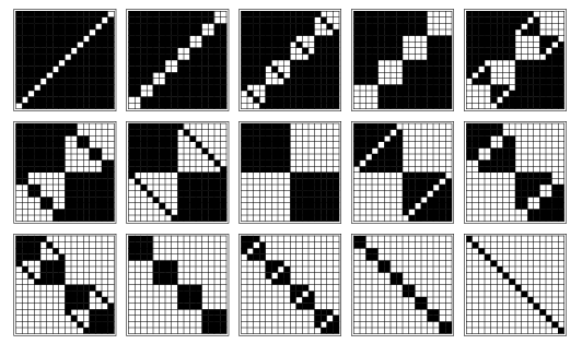
This example code produces a checker board like the one below by XORing two bits in the X and Y coordinates.

Some patterns to try
Munching squares
Munching squares is the Boolean plot x ^ y < t. Where t is time. In this case it would be reasonable to have t take on the values 0..1023. t could be incremented once every frame e.g. when x==799 && y==599.
Varied hue colour gradient
Colours of full saturation and value but varying hue can be generated by varying the red, green and blue according the diagram.
Synthesis vs. simulation
Now you have written some SystemVerilog code to implement one of the options. In the next part of this lab you will see how to use simulation to run SystemVerilog code on a PC or workstation. This has some advantages: the compilation the simulator must do is a lot quicker than the compilation Quartus must do since there is no place & route step for simulation; it is very easy to see values of any variable at any time (a tool called SignalTap provides on-FPGA debug capabilities but they are more limited); and it is easier to write tests for simulation. The clear advantage of synthesis is being able to actually run the full project complete with real I/O e.g. on a demo board. However, in much FPGA development testing using synthesis is merely the final stage after many iterations of testing using simulation. Luckily, for simple projects such as these the advantages of synthesis clearly outweigh the disadvantages of simulation.