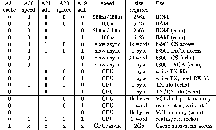
The memory map was selected to require minimal decoding, thus there are many echo access points. The cache subsection takes half of the memory map, being decoded on the top address bit. To enable simple decoding by the timing PAL it was decided that for other accesses the next address bit indicate if a CPU speed or a slow access. Two additional constraints were used, the ROM must be at location zero, since this is the processor reset vector, and following the end of RAM (at its normal address) there should be a read only section. The 68901 implements the 68000 interrupt structure, which requires an IACK cycle in response to an interrupt. To allow simulation of this the address bus is decoded to give both a select and an IACK access route. This gave the memory map outlined in table 1.
The cache has a debug and a normal mode of access, described in section 4. Combining the memory map above with that for the cache gives the base addresses shown in table 2.
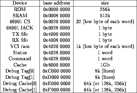
Table 2: Usual Base access addresses