The cache subsystem is selected by the top address bit being set, the next bit is used to select between normal access and ``debug'' accesses. The other address bits are divided into five groups:
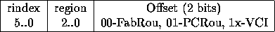
The cache is 2 way set associative, 128k of memory giving 2 x 64k of cache. Each cache line is 32 bytes, to fit into a cell. Thus there are 2k lines in the cache, requiring 11 address bits. The cache tag ram is 8 bits wide, but one of these must be used as a valid bit. This covers 8Mbytes of the address space. This is divided into eight regions as described above. When a cache miss occurs it may be necessary to flush a line, to ensure that only one server needs to be contacted the regions will be separately cached this is referred to as separate regions. This leads to wasting cache space if only few regions are used. The alternative combined regions case makes flushing a cache line potentially more complicated but allows a single region to use all the cache. Experiments should be done to investigate the tradeoff between the two cases, the card will have some links to select between the two. For ARM600 byte addressing table 4 gives the address assignment for 2k cache lines (128k of cache), table 5 for 4k lines (256k) and table 6 for 8k lines (512k). The actual mapping from CPU address to line and tag is done by the ``AdrPat'' selection links, and the selection of the region bits by the ``RegPat'' links. Due to confused thinking the cache controler ``AdrXil'' xilinx also needs to know this mapping so the xilinx bits must match the selectors. Figure 2 shows the pinouts of the selection links, and the correct connections for 256K cache, 2 regions as used in the ``stream cache'' experiments.
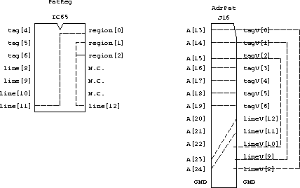
Figure 2: Address Bus to Cache Links
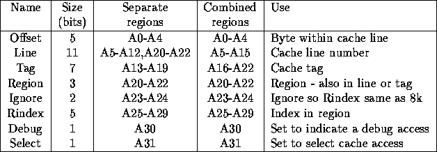
Table 4: Address bit use (2k lines)
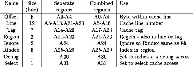
Table 5: Address bit use (4k lines)
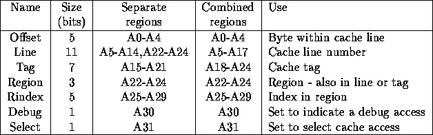
Table 6: Address bit use (8k lines)
Each region of the cache will need an associated VCI. This consists of the fabric and port controller routeing tag and the receiver's association id. This information is obtained from a small dual ported memory. The region number and Rindex bits to index into the dual port memory forming a 10 bit address as shown below.
The Rindex bits are supplied by the MMU when translating a logical address into a cache address. Since the cache resolution mechanism does not take account of the Rindex bits it is possible for several associations to be open in the same region. This would enable (for example) a region to be opened Read-Only and then a write lock be taken out on a small section of it, the region would initially be mapped R/O by the MMU with the Rindex bits setup. When the write lock is taken out (on a new association) the locked pages will be marked R/W, the association table updated and the Rindex translation in the MMU switched. Any data in the CPU cache (accessed by logical address) will still be valid, and any data in the external cache will also be still accessible since the address the cache sees remains the same.
The memory server will have virtual circuits setup with all clients, so sharing will be explicit. Upon detection of sharing the client systems may be informed, and can take appropriate action. This suggests that the server may wish to send updates to clients - this area is still being considered but it is thought that all the extra buffers required are in place. The system may be put into ``flush'' in which any cache line touched that is dirty will be flushed to the memory server.
The ``Debug'' mode of access allows the CPU to read and write the cache memory and the tag memory. This is to allow debugging and the gathering of usage statistics. It will also allow software updates to cache lines. This mode of operation is assumed to be used infrequently and therefore the software will have to perform all the address manipulation itself - address bits are interpreted in the same way as during a standard cache access, for example when accessing the tag rams the tags will be at the 32 byte line spacing apart.. When address bits A31 and A30 are both set the next two bits indicate the device accessed as shown in table 7.
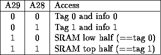
Table 7: Access bits in debug mode
An access to the cache tag memory also accesses the information memory for that line. Ten data bits are used as in table 8.
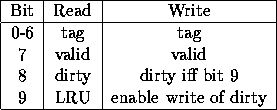
Table 8: Tag and Info data for a line
The tag and valid bits may be read and written. The dirty bit will only be written if the enable bit is set. On a read the top bit indicates which of the sets least (most ?) recently had a cache hit. Accesses to the SRAM in debug mode are 32 bits wide, with the top address bit selecting which bank of the cache is used.
The cache is basically 2 way associative with LRU replacement. This is achieved by storing for each line which set was last accessed (clearly the address for this store is identical to that for the cache tag memory). This LRU data is stored in Info[2]. The output (Q) from this device is passed to the cache controller which uses it when selecting which set to use after a cache miss. A direct mapped cache may thereofe be formed by disconnecting the output from Info[2] (pull it out of its socket and bend the pin!) and pulling the line low causing all cache line fetches to be to set 1. This wastes half the cache, so an alternative is to tie the pin to one of the address bits which are part of the tag field allowing all the cache to be used direct mapped.
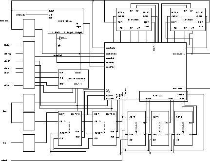
Figure 3: Main parts of the cache
The cache is based around some fast SRAMs and cache tag memories. The tag memories are basically standard SRAMs but if a read cycle is performed with the output disabled the data supplied is compared with the data addressed and a match indication supplied. Two of these devices are used to give a two-way set associative cache. During the `i' (idle) cycle preceding any non-sequential memory access both tag memories perform a match cycle in parallel indicating which half of the cache contains the data or if a miss has happened in addition the information memory for these cache lines is read. Assuming a hit the cache memory is accessed during the `m' cycle, and the LRU and dirty information bits written. If further sequential accesses are performed then the cache memory is accessed again, there is a special case of a wrap over a cache line boundary when a WAIT cycle must be inserted and the tag lookup repeated. The main parts of the cache design are shown in figure 3.
To allow for the cache cycles to be performed at the speed of the processor the logic for performing the tag lookup and the access(es) in the case of a hit is put in the fast timing PAL. In case of a miss a xilinx chip takes over to perform the remote access. There are several reasons for this split. The ARM cycle time is 40ns, and the input and output times of the xilinx would use up a significant proportion of this, using ``10ns'' PALs however the output is valid 7ns after the clock. It seems likely that the `hit' access logic is unlikely to change frequently and using a CMOS erasable PAL will allow easy modifications. The miss logic will involve driving the switch protocol, accessing the cache memory, maintaining the tag memory and holding the VCIs for remote accesses. This will be much more complex logic and is therefore a candidate for a Xilinx chip.
In case of a miss there are two actions that can be taken. The CPU could be stalled (in the case of the ARM600 by stretching the clock cycle) until the old cache line has been flushed and the new one fetched. This stall will last for a large number of clock cycles (especially if the memory server turns the request into an RPC to some other machine) but this is not a problem on the ARM600 which is a fully static design. The alternative is to signal a data abort to the processor, it can then spin polling the memory system but still servicing interrupts that use only local memory. This is an interesting idea, though the ARM600 requires some care to be taken with restarting aborted cycles.
To allow the data abort method, and to allow for cache lines to be updated/invalidated by the cache controller without stopping the CPU, it must be possible to fully isolate the CPU and cache. This cases a few problems as the buffers will add to the delays on data and address paths, but the use of transparent latches should solve this.
The VCI details are stored in a dual ported SRAM. To avoid address collisions the top address bit is generated by a select signal and its inverse. Thus the CPU section can write the VCI table to one half of the memory, and then switch the new table in and the old one out. The switch is done by writing to the control register of the cache subsystem.
The flush-Mode causes a reversal in the operation of the miss control system. If a cache line is hit in flush-Mode then the CPU is halted and the ``miss'' signal asserted allowing the cache controller to access the memory and flush the line. Thus the cpu could flush a region by doing a read for every 32 bytes of the region. A better way to flush a region (given that it is potentially 1Mb and at most 128k could be in the cache) is to use debug reads of the tag ram (a maximum of 2k reads) and flush any lines that are dirty and valid for the region. If a region is being closed then the tag can be marked invalid using a debug write. Flush mode is probably broken by the stream cache modifications to the cdecPal. The pin used to pass the information in has been stolen for other uses. It is probably possible to put flush mode back (using Al[29] in the cdecPal) - see the PAL equations and the RCS log.
Timing information may be extracted from the cache section. The ``miss'' signal indicates when the CPU is stopped due to a cache miss. Pin 22 of the time2Pal toggles on every access to the cache - i.e. using it to clock a counter gives half the number of cache accesses. Care is taken to ensure sequential accesses are counted correctly even if they cross cache line boundaries (read the equations).