The ARM600 is rated up to a core clock (FCLK) of 25MHz. It is usual
for the memory clock (MCLK) to be approximately half this speed. The
processor switches between the two as required. Since the main point of
the processor node is investigating the use of the external cache it has
been decided to run the memory clock at the same speed as the core. This
is permitted by the original data sheet![]() , although it changes some of the assumed
phase relationships between signals. Using processor synchronous mode
should ensure no penalty in switching between the two clocks.
, although it changes some of the assumed
phase relationships between signals. Using processor synchronous mode
should ensure no penalty in switching between the two clocks.
The use of a fast external clock for the processor requires that wait states be inserted in accesses of all the local memory and devices. This is done by a PAL and a fast gate which will assert the nWAIT signal on every memory cycle where required. A cache access, in the event of a hit, is performed at CPU speed. The control section of the cache subsystem and the perhaps interface also work at CPU speeds. Local memory is slow, SRAM having 100ns access time, and ROM 150ns or 250ns. The 68901 uses the 68000 asynchronous bus protocol, based on a 4 MHz clock, providing an acknowledge to terminate an access after approx 250ns plus the clock synchronisation time. The timing PAL decodes the top two address bits and the cache hit signals to determine whether to signal a WAIT as shown in table 3.
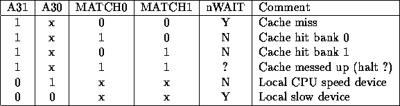
Table 3: Decode for nWAIT insertion
The reset system uses a pal to count 4 MHz clock cycles to provide a valid reset pulse for all devices on the card. There are four sources of reset: the front panel switch, the fabric, the watchdog timer and the cache controller. The first two are as for port controllers. The watchdog reset is provided by the output of a timer register and enables resetting of the machine if some number of regular timer interrupts are missed. This feature has proved useful on the 68k Wanda systems, and is a link option on the MDH-9. The cache reset line is provided to enable the cache controller, or possibly reception of a control cell, to reset the card, this is programmed by the xilinx design. The reason for the last reset is available through the 68901 I/O lines as described later in table 13. There is an outstanding problem with reset. The ARM 600 counts on the address bus while in reset, and performs two memory accesses to the next two locations on coming out of reset - if these are to an unfortunate location the nWAIT signal is asserted and the CPU will hang. This can probably be cured by ignoring these cycles but this has not yet been done.