Registers


Next: ARM accesses
Up: FPC2 xilinx chip -
Previous: The queue
The new xilinx chip has more registers than the previous version,
some of these may be read and written by the processor. There are
no checks that the processor is putting sensible values into the
registers, or that writes are done at sensible times. The registers are:
- ArmP.
- Points to the start of the queue structure. Buffers
between ArmP and HeadP are ready to be collected by the processor. Can
be read and written by processor, optionally reading may have the side
effect of stepping it on to the next buffer in the queue if ArmP !=
HeadP.
- HeadP.
- Points to the head of the free queue, and the cell
that is currently being received. May be written by the processor.
After a cell has been received HeadP steps on to the next buffer in
the queue.
- TP1.
- Points to the last buffer in the free queue - the
transmit queue hangs off the link pointer of this buffer. May be read
and written by the processor. If HeadP becomes equal to TP1 then the
free queue is empty and an interrupt raised. While the free queue is
empty cells will only be read from the RxFifo, any cells read will be
discarded and the TOG status bit set.
- TransP.
- Points to the buffer being transmitted, or that
has just been transmitted (if there are no more to send). When this
register is updated by the xilinx its old value is moved into TP1. May
be written by the processor with no effect on TP1. TransP is advanced
just before sending a cell (unless the cell is being automatically
retried). After a NACK causing the retry limit to be reached TransP
will point to the cell NACKed, and transmission will stop. To restart
discarding the NACKed cell a ``GoTx'' command should be issued. To
restart with further retries TransP should be loaded with the value
read from TP1 and CNT incremented before the ``GoTx'' command.
To reorder the transmit queue the new queue should be built under the
link pointer from the buffer pointed to by TP1 and TransP written with
the value from TP1 - note that since TP1 is unaltered by processor
writes of TransP it will remain valid even in the case of an immediate
NACK. TransP, and thus the cell link pointer, also contains two
control bits local which when set prevents VCI remapping taking
place
 and NoTx
which marks the cell for dummy transmission. A dummy transmission
returns the cell buffer to the free queue by passing it through the
transmission machinery without injecting it into the fabric - this
still takes a whole frame period.
and NoTx
which marks the cell for dummy transmission. A dummy transmission
returns the cell buffer to the free queue by passing it through the
transmission machinery without injecting it into the fabric - this
still takes a whole frame period.
- Remap.
- The remap register is internal to the xilinx and
provides a temporary store for the VCI used in a VCI remap operation.
The remap register is short lived, and relies on the pipeline for the
correct address to be formed.
- CNT.
- The CNT register stores the number of outstanding
transmission requests, ie the number of valid buffers after TransP.
The processor may increment the count as a side effect of writing
memory or registers. The transmit available interrupt is raised if the
count is less than 8, the counter will not increment if this is not
the case. This is done to restrict the fifo queueing in hardware to 8
buffers, allowing software control of larger queues.
- Command.
- The command register is writable by the processor
to issue commands to the xilinx chip. These currently consist of
``goTx'' which starts the transmission system (this replaces
pulsing the ramRdGo signal), and ``RqW'' which requests a buffer from
the free queue for use by Wanda. These two commands are both initiated
by writing the command register with a particular bit set, these bits
are not stored so there is no need for the set-wait-clear that was
required on the previous version of the chip. A buffer request from Wanda is
serviced whenever the receive system is looking for a start of cell. A
cell for Wanda has the timestamp put in words 0 and 1 of the buffer,
thus ensuring that bit 15 of the VCI is set so it can be recognised.
Only one request may be outstanding at any time, so Wanda should wait
for one to be serviced before issuing another, or regard the request
as an unreliable operation.
- TimeStamp.
- The TimeStamp register is inserted in word 0 of
a successfully received cell buffer just prior to advancing HeadP -
this happens whether the buffer was truly recieved or was requested
by Wanda. The TimeStamp contains an 11 bit count, which increments
every fabric frame pulse (ie 64 clock cycles). The top two bits
indicate the source of the cell (for Wanda, rx fifo, loopback fifo)
to assist debugging. Also the ``latched status'' bits are inserted for
reasons that I don't propose to go in to! (Actually these may be useful
for debugging too). Bit 15 of the TimeStamp is always 1, so that the
timestamp can be used as the ``VCI/FAS'' word for cells to Wanda. If
the timestamp is read by the processor (rather than being read
indirectly via a recieved cell) the source information will probably
not be useful since it is only valid when a cell is actually being recieved.
- Status.
- The status register is read only and can be read
with either ArmP or TP1. Most of the bits in the status register
record conditions that have been seen by the xilinx, these are latched
until a status-read-and-clear is done (allowing low level
software to examine the status but only higher levels to record
details). It should be noted that a cell timeout (TMO) error is likely
to provoke stray bytes (BYT), and a cell thrown on
ground (TOG) error will always provoke stray bytes.
- IrqStat.
- The IrqStat register is read only and can be read
with either ArmP or TP1. When read with ArmP there is an option to
cause ArmP to follow the link to the next cell buffer. This reload
will only happen if ArmP != HeadP (ie there are cells to collect). The
information in IrqStat is an expanded form of the interrupt request
lines presented to IOC, thus after an interrupt one read will get both
the reason for interrupt and collect the buffer if it was a receive
interrupt.
Figure 3 shows the format of the various registers. The
xilinx chip has no access to data bits 16..29 so these are undefined
on read and may be written with any value.
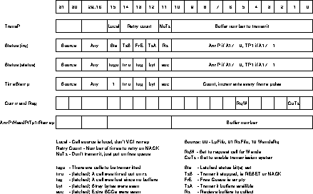
Figure 3: Transmit buffer pointer and status regs.
Next: ARM accesses
Up: FPC2 xilinx chip -
Previous: The queue
Mark Hayter and Richard Black