contents | 1-overview | 2-background | 3-results summary | 4-results details | 5-deliverables | 6-dissemination | 7-conclusions
We produced two variants of the XAP
16-bit microprocessor: a conventional fully-synthesised clocked version and a
secure dual-rail asynchronous version. Both designs used a conventional ASIC
design flow for the low level aspects of the design and were integrated onto one
0.18um CMOS test chip code named Springbank. This provided us with a
unique opportunity to make a side by side com
The Secure XAP includes a bus cryptography unit (designed in conjunction with Cryptomathic) so that only encrypted data is written to memory. The Springbank test chip also includes on chip memory (SRAM) and distributed asynchronous interconnect. It also has an I/O block which includes RS232, smartcard and parallel interfaces.
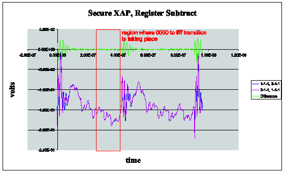
The Secure XAP has demonstrably lower data dependent power emissions than the conventional synchronous counterpart. See Figure 1 and Figure 2 below for an example of differential power analysis when performing a subtract on the two processors. For these experiments, data was collected from the same program but with different data (for the subtract operation) which is shown in the magenta and blue traces. These signals were obtained after 4000 cycles to reduce noise. The difference is in green. You will see that there is negligible power difference for the two runs. Thus, it is far more difficult to undertake a differential power analysis (DPA) attack on the secure XAP. Further details are available in a paper published by S.W. Moore et. al, Balanced Self-Checking Asynchronous Logic for Smart Card Applications, to appear in the Journal of Microprocessors and Microsystems. Earlier work appeared in a paper by S.W. Moore et. al, Improving Smart Card Security using Self-timed Circuits, Proceedings of the Eighth International Symposium on Asynchronous Circuits and Systems (ASYNC 2002), IEEE Press, March 2002.
During the G3Card project, ElectroMagnetic emissions Analysis (EMA) techniques were refined. It was discovered that the Secure XAP was susceptible to this attack in much the same way as the conventional synchronous XAP. Our improved understanding the EMA technique has allowed us to investigate countermeasures.
Optical fault injection attacks have also been tried on the Secure XAP. The dual-rail encoding scheme successfully detects many attacks. Where full dual-rail encoding was not adhered to, the circuits could be broken. However, full dual-rail encoded circuits were demonstrated to work very well.
The areas where the Secure XAP was vulnerable were primarily due to small implementation oversights which did not impact the functional correctness. Thus, it became quite apparent that we needed to be able to include security validation criteria as part of the design time validation process. Thus, work towards the end of the project focused on design time security validation.
Figure 1 Secure XAP, Register Subtract
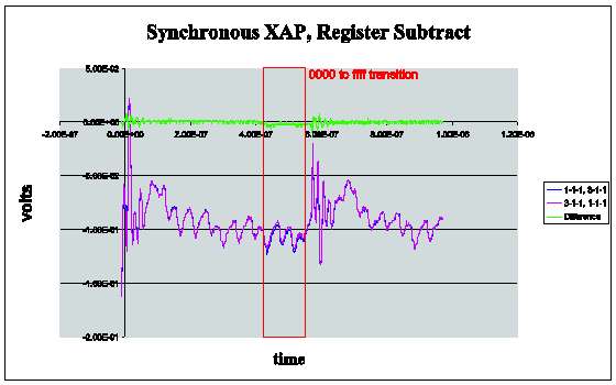
Figure 2 Synchronous XAP, Register subtract
The prototype asynchronous SmartMIPS™ developed in this
project was integrated into a Testchip fitted onto an evaluation board bearing
the basic needs for carrying out tests. Due to time restrictions only one part
of the SmartMIPS™ was actually implemented into asynchronous technology. We
chose the MDU because it is an important part in the MIPS4Ksc™ architecture. It
is the block which performs, for example, the multiplication instructions so
heavily used for Public Key Cryptography. Apart from the MDU, the rest of the
SmartMIPS™ was implemented in the ‘conventional’ clocked scheme. We also kept
the synchronous MDU so as to allow fair com
· Implementation of an asynchronous MDU using Tima’s in-house design methodology for implementing secure asynchronous logic
· Implementation of the mixed synchronous/asynchronous/synchronous interface to support communication between the rest of the processor and both the synchronous and asynchronous MDUs.
The resulting Testchip was shipped in September 2002. It was successfully validated before shipment to our partners (NDS and UCL) for evaluation.
The Amulet group's contribution to the G3Card project was to fabricate a completely new processor design based on the established ARM architecture. Priority in design was given to making the chip as secure as possible from non-invasive attacks attempting to determine the data being processed.
The design of a completely new custom chip using a conventional approach was infeasible within the resources available to the project; the decision was therefore made to employ Balsa, an asynchronous system design tool set, which was in the process of development within the Amulet group. This required significant refining of the tool set and rewriting of its back-end to make it suitable for the security-oriented target circuits designed for the smartcard prototype processor core SPA (Synthesised Portable Amulet).
A set of secure logic gates and storage elements was designed which minimised the variation in supply current which occurs when a CMOS circuit switches from one logic state to the other and which balanced as closely as possible the input to output delay variation depending on input signal combinations. Dual-rail encoding was used throughout the processor core to ensure a constant Hamming weight for all data fields. Additionally, storage elements were organised so that their contents were always returned to a null state prior to loading so that the loading of a new value always results in a logic value change in each bit thus minimising data dependent variations.
Two SPA processor design
implementations were integrated with memory systems, a UART and other ancillary
units interconnected by Chain, the self-timed Network-on-Chip, also developed
within the Amulet group. The security oriented dual-rail, secure latch processor
core which had been the focus of the design effort was the processor destined
for smartcard applications; the other processor was synthesised from the same
specification but implemented as a single-rail bundled-data design. Having both
processors available on the chip made possible com
The decision to employ the experimental Balsa tools proved to have been correct; the design was completed and simulated well within the required timescale. The G3Card chip was fabricated through the MOSIS service using a TSMC 0.18μm 6 layer metal process which runs the core cells at 1.8V and the pad ring at 3.3V. The prototype chip occupies an area of 33mm2 and incorporates the two versions of the SPA processor, 192 Kbytes of RAM, 256 words of ROM and several peripheral and experimental devices. The chip samples were shipped by MOSIS in October 2002.
Basic power and timing analyses were conducted to obtain initial indications of the effectiveness of the secure design methodology against non-invasive attacks. Five different instructions were selected as targets for power and timing analysis: ADD, BRANCH, MUL, SHIFT and XOR. These instructions are commonly used in cryptographic algorithms and are deemed the most likely to leak information through varying power consumption or timing.
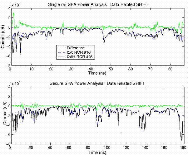
Figure 3 Single-Rail and Secure SPA Power Traces
Figure 3 shows power traces for the execution of a SHIFT instruction. The upper window corresponds to the single-rail SPA. The darker traces correspond to executions of the same instruction with a different shift distance. The lighter trace corresponds to their difference. The lower window shows equivalent traces for the secure SPA processor. Clearly, the difference trace is much larger for the single-rail SPA, indicating that more information is leaked.
Several experiments were conducted to evaluate the maximum potential side-channel leakage. In each experiment a single instruction was targeted using only two different data values. A successful extraction indicates that the correct value of the data was extracted from the trace. The Probability of Correct Deduction (PCD) is defined as the percentage of correct deductions in a set of experiments.
|
ARM Instruction |
Single-Rail SPA |
Secure SPA |
|
|
|
Simulated (%) |
Simulated (%) |
Measured (%) |
|
ADD |
100.0 |
78.0 |
79.9 |
|
BRANCH (conditional) |
100.0 |
100.0 |
100.0 |
|
MUL |
100.0 |
85.1 |
68.5 |
|
SHIFT (varying distance) |
100.0 |
100.0 |
81.9 |
|
SHIFT (varying data) |
100.0 |
65.0 |
60.3 |
|
XOR |
100.0 |
67.0 |
61.3 |
Table 1 Power Analysis: Probability of Correct Deduction
Table 1 shows the results for the different instructions analysed, both for the single-rail and the secure SPA cores. A PCD of 100% indicates that the differences in the power consumption signature are considerable and data can be deduced easily. A PCD of 50% suggests, in these two-valued experiments, that no information is forthcoming and deduction is essentially random.
The results shown in Table 1 are very encouraging. The single-rail SPA simulations show that 100% correct deductions can be obtained in every case, indicating poor resistance to power analysis. By contrast, the secure SPA yields much lower PCDs in most cases, both in simulation and in actual measurements. However, the analysis also shows that the BRANCH instruction is vulnerable in the secure SPA and should be corrected in future designs.
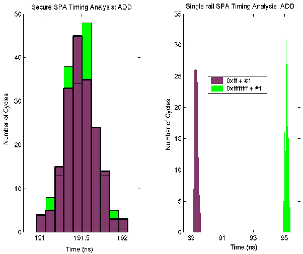
Figure 4 ADD Instruction Timing Analysis
The same experiments were used to perform timing analysis. Figure 4 shows the results generated in the experiment targeting the ADD instruction, the secure SPA on the left and the single-rail SPA to the right. The x axis displays the range of times which each SPA takes to execute the instruction and the y axis indicates the number of cycles which fall into the respective bins. The darker bars in each chart show the execution of an ADD instruction which causes an 8-bit carry propagation and the lighter bars show those for a 32-bit carry propagation.
The figure clearly shows that the two sets of bars are almost fully overlapped for the secure SPA indicating that using an ADD instruction to process two different data values takes almost exactly the same time to complete (average 191.5 ns). In contrast, the two sets of bars are disjoint on the chart for the single-rail SPA. The times fall into two separated groups, one averaging 89.3 ns and the other 95.1 ns. The difference between the two average times is about 6%. The larger variation indicates that the single-rail SPA leaks information much more severely than does the secure SPA.
|
ARM Instruction |
Single-Rail SPA |
Secure SPA |
|
|
Simulated (%) |
Simulated (%) |
|
ADD |
100.0 |
51.0 |
|
BRANCH (conditional) |
100.0 |
100.0 |
|
MUL |
91.8 |
76.1 |
|
SHIFT (varying distance) |
100.0 |
100.0 |
|
SHIFT (varying data) |
100.0 |
51.9 |
|
XOR |
100.0 |
60.0 |
Table 2 Timing Analysis: Probability of Correct Deduction
As for power analysis, the probability of correct deduction (PCD) is used to evaluate the success of the analysis. Table 2 shows the timing analysis results for the instructions targeted by the experiments. These results confirm that the single-rail SPA has poor security against timing analysis, since all instructions result in 100% correct deductions (with the exception of MUL, which is very close at 91.8%). These results highlight the significantly improved security of the secure SPA for most instructions, particularly ADD and XOR. The results also show that the BRANCH and SHIFT (varying distance) instructions are vulnerable in the secure SPA and this aspect should be addressed in any future design.
Further experiments were conducted to evaluate the impact of the different security-enhancing techniques used in the design. The same experiments mentioned earlier were repeated using the secure SPA with the configurable latches set as conventional (insecure) dual-rail latches.
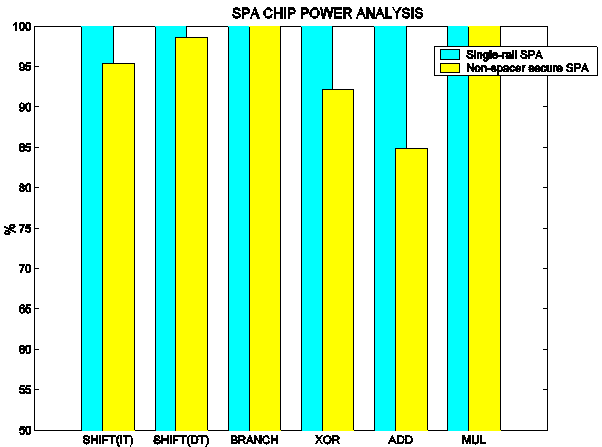
Figure 5 Impact of Dual-Rail Encoding: Probability of Correct Deduction
Figure 5 shows the power analysis PCDs for all the instructions targeted in the experiments. The dark bars correspond to the single-rail SPA and the light ones correspond to the secure SPA with the conventional dual-rail latches. These results show the impact of the use of dual-rail encoding without secure latches.
Clearly, the dual-rail SPA has better PCD ratings in most cases, with improvements ranging from 2% to 15%. However, these results show that the use of dual-rail encoding alone is not likely to produce circuits with adequate security.
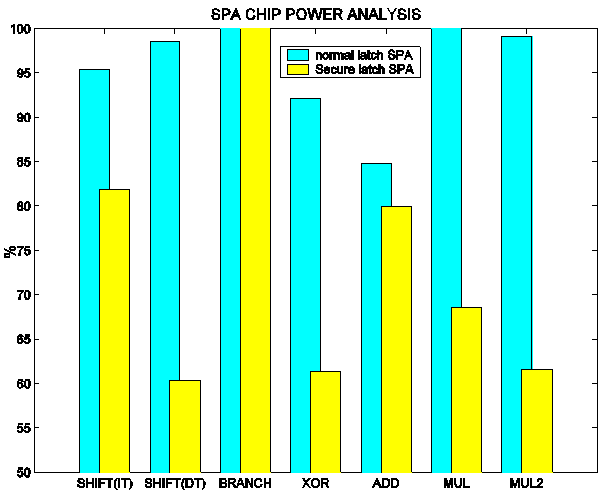
Figure 6 Impact of Secure Latches: Probability of Correct Deduction
Figure 6 shows the power analysis PCDs for the secure SPA with the two different types of latches. The dark bars correspond to the conventional dual-rail latches while the light ones show the results of using the secure dual-rail latches. Clearly, the secure latches have a large impact on the PCD, indicating that their use can result in significantly enhanced security. The figure also shows that the SHIFT (varying distance) and ADD instructions did not benefit as much as the others, which requires further investigation.
In conclusion the Amulet G3Card contribution has been to demonstrate the feasibility of using synthesis techniques to produce a commercial smartcard processor design with improved resistance to non-invasive attacks. An analysis of the probability of distinguishing different data fields being processed in the secure chip compared with that for a conventional design clearly shows the benefits of the secure circuit design.
The Cambridge and
|
Dual-rail Signal |
Symbolic Meaning |
|
00 |
Clear |
|
01 |
Logic-0 |
|
10 |
Logic-1 |
|
11 |
Alarm |
During conventional operation circuits move from the Clear state to the Logic (0 or 1) state and back again. Injection of a fault will have one of the following results:
· A Logic state turns into an Alarm state raising the alarm
· A multiple fault causes a Clear state to turn into an Alarm state
· A Logic state turns into a Clear state which results in deadlock
· A Clear state will be turned into a Logic state which also results in deadlock
The Springbank test chip (see Section XAP designs) embodied a processor constructed using these techniques. We were able to demonstrate that these dual-rail circuits inhibited fault injection which was useful to an attacker.
Dual-rail circuits have also been demonstrated to produce substantially less data dependent power since the transitions between Clear and Logic states can be made to consume constant power.
The implementation approach taken by Cambridge was to hand craft much of the design. This reduced the CAD tool effort and allowed the relatively simple 16-bit processor designs to be completed for early evaluation.
The
Further results, circuit level details and validation approaches may be found in the publications listed at the end of this document.
It is common for security evaluations of hardware to be undertaken after the device has been manufactured. This is a time consuming, expensive and error prone process. None the less we have recently trodden this well travelled path to produce a test chip (Springbank) and evaluate it. The design and evaluation of the Springbank test chip has taught us a great deal about the typical smart card design process. We began this process in the traditional way with a requirements specification which included security properties. This lead to us identifying key design criteria which steered the design process. However, we lacked design time validation of the security criteria and we now know that some side cases were overlooked. Even more worryingly, our colleagues working on attack technologies developed new attacks which we had not even considered during the design process. What we seem to have recreated in our research project is a microcosm of current industrial practice.
Having analysed security attacks on our circuits, we have been able to devise validation techniques which may be used at design time.
Power Analysis:
G3Card has been very focused on power analysis attacks. We have determined that
data dependant leakage may be detected at design time via systematic
simulation. Such simulations allow design com
Fault Injection Analysis: Injecting faults into working processors can change the nature of data being treated or corrupt cryptographic computations in such a way as to unveil secret information. Early forms of these so called active attacks were focused on the device's external interface and often involved introducing glitches on power or clock input pins {AndKuh96}. Changes in temperature, either by cooling or heating the whole device or the introduction of a temperature gradient, may also be used to induce faulty behaviour. Defences against such attacks are simplified by the restricted nature of the channel by which faults are injected and can easily be detected by incorporating a suitable tamper sensor. Far greater control over the nature of the faults injected has been demonstrated recently. These attacks have included the use of localised EM pulses (by UCL), laser light, X-rays and local heating. We have been able to model this range of physical phenomena which can trigger faults. We can then model a wide range of attack scenarios from single to multiple transistors failures. Given bounds on the control the attacker has, we can determine whether a fault can be injected without being detected.
Our long term aim is to produce a validation suite which covers a range of fault induction and measurement possibilities which far exceeds current known attacks. Using this approach we believe that security by design will become a far more powerful technique than security analysis post manufacture.
The smartcard processors developed in this project incorporate fine-grain memory protection units. This hardware improvement can potentially improve the security of smartcard applications in several areas:
· Resistance to glitch attacks; these rely on stressing the processor physically to cause it to execute an instruction in a faulty manner. For example, the “test” operation at the end of a loop that is reading out memory may be skipped, causing the loop to be executed extra times and exposing the contents of more memory than was intended. If the memory protection unit is always set to the “most restrictive possible” state then this kind of attack is made much harder: not only must the correct instruction be glitched, the attacker must also find a way to disable the memory protection unit or arrange for it to be programmed incorrectly.
· Resistance to application programming faults; application programming errors that might previously have gone unnoticed, for example an access to an “unallocated” area of memory, will now be trapped automatically and will cause the application to fail. The application programmer can correct errors that are caught in this way during development. Errors of this type that remain in the finished application will cause the application to fail when they occur, but should not affect the security of the card.
· Separation of applications into mutually-suspicious components. The parts of the application that deal with issues like communication with the card accepting device and dealing with external requests can be completely separated from parts of the application that deal with encryption and key management. Communication between these parts can take place across a well-defined internal interface, with checking on both sides: the part that deals with access to key material can have an internal policy that it will not perform operations using a stored key unless a correct PIN has been presented, and will refuse to do so even if asked to by the component that implements communication with the outside world.
· Separation of mechanism and policy. Applications can be written to provide mechanism, for example performing operations using stored key material. Policy about what to permit the application to do can be implemented in separate code that does not have access to the application’s internal data.
A further benefit of having a fine-grain memory protection unit is that multiple applications, written in the smartcard processor’s native machine code, can be supported on the same card without having to trust each other.
The benefits listed above all derive from the presence of a memory protection unit, but this hardware requires careful management in order to deliver the benefits in a safe and usable way. The project has developed an operating system that provides this. The operating system consists of a small supervisor that runs when the card is reset, and a number of user-space modules. The supervisor is responsible for low-level management of the MPU (and some other hardware resources, for example the countdown timers). It provides protection-related services to the user-space modules and uploaded applications.
The key concept supported by the supervisor is a protection domain (“domain” for short). A domain consists of a list of memory protection requirements: regions of memory and their accessibility. The supervisor programs the MPU to meet these requirements (dealing with the limited resources of the MPU by swapping protection regions in and out as necessary). Domains also contain some ancillary information: the address of a routine to call when a protection fault occurs, an execution time limit, and so on. When the card is reset, the supervisor creates a domain that allows access to all of the resources on the card, and runs the ‘init’ module.
On its own the concept of a domain is not terribly useful. However, the supervisor does not just support one domain at a time; instead it supports a stack of domains. The current domain is the one most-recently pushed on to the stack; the supervisor programs the MPU only to allow accesses that are permitted by the current domain and all other domains on the stack as well. Domains are exposed to user-space by a system call that allows the currently-running user-space code to push a new domain onto the stack. This allows user-space code to produce new execution environments that are more restrictive than the current one, and never less restrictive.
When a protection fault occurs in the current domain, the supervisor pops it from the stack and calls the address specified in the domain descriptor. This enables the “parent” of a domain, if it wishes, to handle faults that occur in that domain. This mechanism can be used for a number of different things; the trivial case is that the child domain faults deliberately when it wants to return control (and a result) to its parent. Faults also occur when the time limit assigned to a domain expires; in this case the parent can decide whether to allocate more time to the domain, call a different domain (enabling a simple kind of pre-emptive multi-tasking managed entirely in user-space) or give up and deal with the event as an error.
If the parent is unwilling to handle the fault then it is propagated up the domain stack until a domain is found that is willing to handle it. If the fault reaches the top of the stack and is still unhandled, the supervisor freezes the card; this is clearly an error condition.
Domains can request services from their parents (and indirectly from the rest of the operating system) by executing a software interrupt instruction. This causes a fault that their parent (or parents’ parent, or whatever) can handle, perform an operation (that might involve starting other domains) and eventually return control to the domain. Parents can define any set of services they like to provide to their children in this way, and can also mediate access between their children and the rest of the operating system.
The user-space section of the operating system has a fairly simple structure. As mentioned earlier, the first user-space code to be called after card reset is the init module. This creates domain descriptors for its immediate children: the “comm” module that deals with communication with the card accepting device, the “rng” module which manages the card’s random number generation hardware, the “nvr” module which manages the non-volatile storage on the card, and the “app” module which manages all the installed applications on the card. There are a number of libraries that provide cryptographic and utility routines; these are called directly by application code (usually in a sub-domain to protect the application against faults in the library code and to ensure that the library routine has access to as little of the card’s resources as are required for it to complete its task).
Init has access to all the resources of the card, and so is kept very simple with static memory allocation and static policy. Its main job is to pass requests between app and the other modules. Its only important policy is over ownership of the APDU buffer, the area of memory used to pass APDUs between the comm and app modules; both of these are allowed access to the buffer, but only one of them at any one time.
The app module is the most complex of the OS-provided modules. It keeps data relating to all of the uploaded and instantiated applications. When an APDU arrives from the card accepting device, it is passed to app which inspects it; if it is a SELECT APDU then app consults its list of applications, starts up the appropriate one (in a sub-domain) and passes further APDUs to it. App provides a number of services to applications; it mediates inter-application calls, and it enables applications to access their own areas of non-volatile memory.
App itself is policy-neutral; its default policy for all operations is just to do them. More sensible policies can be specified in a special “policy application”. This is uploaded to the card like any other application, but instantiated using a special call to app. Once a policy application is installed, app will consult it before performing any operation (including allowing the upload of new applications, deleting old applications, permitting any inter-application call, and allowing any allocation of non-volatile memory). The ability to specify card policy safely in native code gives G3CardOS great flexibility; for example a “transport key” feature could be included in cards at manufacture time that prohibits the upload of new applications until a key is supplied to the card.
Elliptic curves
Elliptic curve algorithms are emerging as secure and efficient alternatives to the RSA algorithms. Several standardization bodies (e.g. IEEE) are working on cryptographic protocols using elliptic curve cryptography.
Elliptic curves are defined by an equation of the following form, over a finite field:
y2 = x3 + ax + b (mod q)
Here q is an odd prime power. Elliptic curves can also be defined over fields with an even number of elements. Then, an equation of the following form is used:
y2+xy = x3+ax+b (mod q)
Here the operations “+” and “.” are not ordinary integer arithmetic, but operations over the finite field.
The points on the curve, i.e. the pairs (x,y) satisfying the equation, together with a special point at infinity, form a group.
The main attraction of elliptic curve cryptosystems arises because the analogue of the discrete logarithm problem on these curves is apparently much harder than the discrete logarithm problem in Z^*_p and the integer factorization problem.
Consequently, in elliptic curve cryptosystems the same level of security can be obtained working in much smaller fields.
Point counting
The generation of suitable elliptic curve parameters is the major obstacle in an elliptic curve environment. In order to resist known attacks, it is required that the number of points on the curve should not be smoothly factorizable. The most popular way to achieve is, is by generating a random curve and determining (“counting”) the number of points on it.
Advanced mathematics seems to be required in order to determine the number of points efficiently.
A completely new algorithm, for counting points on elliptic curves over finite fields of small odd characteristics, has been discovered by T. Satoh. It uses a lot of the arithmetic of elliptic curves such as lifting to characteristic 0, small Frobenius maps, isogenies, p-adic numbers and trace calculations. The original Satoh method doesn’t work for curves over fields with an even number of elements.
Cryptomathic has managed to develop an algorithm that solves this problem.
Because smartcards have constraints on memory size and code size, and will remain to have them in the foreseeable future, this new counting method was revised to become better suited for these restrained environments.
Software countermeasures against side-channel attacks
Also during this project, we studied software countermeasures that can be taken to protect cryptographic protocols using elliptic curve cryptography. These software countermeasures can be used on top of hardware security measurements.
The countermeasures described in the literature were classified according to the level on which they operate. Some examples of the countermeasures we studied are: different techniques for masking points and scalars, the use of randomized projective coordinates, unified addition formulas. We generalized some of the countermeasures. Secondly, the resulting decrease in performance of the different countermeasures was compared. We also studied the counterattacks that were proposed in order to circumvent the countermeasures.
Conclusion
During this project we developed efficient algorithms and implementations for generating cryptographically secure elliptic curve parameters in a smartcard environment.
We also investigated the security of cryptographic protocols based on elliptic curve cryptography, and how software techniques can complement the hardware security to achieve maximal resistance against side-channel attacks.
At the time this report has been handed in, tests were completed on the XAP processor and on the SmartMIPS. The first of those two chips under test was the XAP processor designed by the University of Cambridge. The Springbank chip consisted of several versions of the same 16-bit RISC processor, one of which is a ‘conventional’ clocked circuit (the SyncXAP) and one other being the SecXAP, a dual rail with RTZ asynchronous circuit. With those two processors, we carried out comparative tests based on four attack techniques.
Power Analysis showed that both the SyncXAP and the SecXAP leak information through Hamming weight current consumptions. However, it is shown that for the asynchronous circuit, this power signature is reduced by a few dB. The principal reason for the persistence of information leakage in the SecXAP is proposed as being due to design issues where the automatic place&route tools used produced wires of uneven, unbalanced lengths.
Electromagnetic Analysis yielded the same kind of results as for the Power Analysis, except that the SecXAP seemed to radiate off more significant information, which is probably due to the larger circuit size, the absence of the ‘noisy’ clock and to unevenness due to automatic place&route.
Light/Laser fault injection unveiled weaknesses in the SecXAP’s design as explained earlier but apart from those local fatalities, the rest of the circuit went into a ‘stall’ state whenever submitted to such aggressions.
Vcc glitches on the SecXAP unfortunately turned out to be as fatal as it is on the clocked version of the processor, producing exploitable faulty behaviours.
The second chip was based on the SmartMIPS™ architecture. The Silicon Design team of Gemplus designed the Testchip upon which the tests were carried out. The core is a clocked one with two different versions of the multiplier: the normal clocked multiplier (the SyncMDU) and the asynchronous secure multiplier (the AsyncMDU). At the time of this report, only Power Analysis had been performed to compare the two multipliers. We ended up confirming the results obtained on the XAP processors: i.e. Information leakage on the asynchronous MDU is lower, but still significant, than on the clocked MDU by a about 20 dB.
The general conclusions that can be drawn from those tests are the following: the dual rail with RTZ asynchronous technology does reduce power dependant information leakage by a few decibels. More significant reductions in the information leakage could have been achieved by having appropriate design tools or by doing careful full custom chips. Moreover, those design weaknesses also have a dramatic impact when it comes to injecting exploitable faults. This also means that the task of protecting a chip against fault injections is far from being that simple and that there is still plenty of room left for further research.
The team at Cambridge worked first on the problem of data retention in semiconductor memory. It is commonly assumed that once power is removed from a static RAM, the memory contents are immediately destroyed. This is not the case. The data may remain readable for several seconds, in that the device will revert to its former state if powered up again. If the chip is frozen, this remanence period may increase to minutes or even hours. The existing views of the security engineering community rely on papers published in the 1980s, when technologies were very different. We considered it important to repeat this work using modern components and we found a wide variation in remanence behaviour, even between different devices of the same type and from the same manufacturer.
The team at Louvain-la-Neuve started off refining their work on electromagnetic analysis. This technique involves placing a small probe coil on the surface of the chip under test and measuring the current induced in it by the local magnetic field at the chip’s surface. In some circumstances, this gives similar information to that obtained by measuring the chip’s power consumption (i.e., in power analysis). However, it was shown that electromagnetic analysis gives strictly more information, as the coil can pick up the magnetic fields generated by local signals that are not present outside the chip. This was highly significant in itself; it also turned out to be important for later analysis and protection work.
The Cambridge team then turned to optical fault induction. This work started by chance, with the observation that the microscope light caused a short-circuit in the EEPROM read-out amplifier of an SLE66 smartcard that was under test. This led the Cambridge team to wonder whether it would be possible to induce a fault in the component of their choice by illuminating it. A second-hand photographers’ flashgun was purchased and mounted on a microscope; it was found that suitably aimed flashes could be used to write arbitrary values into SRAM. This result got considerable publicity. The use of lasers rather than flashguns enabled the technique to be made more precise and to be extended to smaller feature sizes.
The team at Louvain-la-Neuve then developed a variant of this technique using their electromagnetic probing tools. By placing a small coil next to a target component in a smartcard chip, and passing a current pulse through the coil, they found that they could induce a sufficiently large eddy current in the chip to cause a targeted malfunction.
The final attack technology development brought Cambridge and Louvain together, to explore new ways of recovering data directly from semiconductor memory without using the read operations provided by the chip vendor for that purpose, thereby circumventing any access controls and reading out secret data directly. This is also a semi-invasive attack, in that the chip is still de-packaged, but no direct electrical contact is made and the chip passivation remains intact. We will describe the technique in the context of an optical attack on CMOS RAM, but it has much wider applicability; electromagnetic probing techniques work too, and many other types of memory are vulnerable.
The structure of a typical SRAM cell is shown in Figure 7. Two inverters are built from pairs of p- and n-channel transistors. The output of the first inverter is connected to the input of the second, and vice versa. Two n-channel transistors are used to read data from it and write data into it.
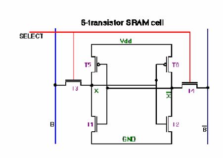
Figure 7 The architecture of an SRAM cell
To read out this memory cell, we used a red laser focused on the chip surface using a microscope. The photons (650nm wavelength) ionise active areas inside the chip. If they strike an area near a p-n junction, a photocurrent will be produced. The decrease in resistance is noticeable for closed channels, and almost negligible for open channels. Thus, by aiming the laser beam at an appropriate transistor or transistors, we can distinguish between the two possible memory states.
In our first experiment, we built a map of the active areas in a microcontroller by measuring the photocurrent induced by laser scanning the chip surface. The chip was mounted on an X-Y motorized stage with 0.1μm resolution. The result of the scan is shown in Figure 9. The active areas can be seen as they produce higher current, but most of the chip is covered with metal layers which the laser cannot penetrate, so these areas do not produce any current. We used this picture as a reference to the results obtained from a powered chip.
Our next experiment was done with an operating chip. It was programmed to allow us to upload any value into its RAM and then stop the chip operation. The result of the scanning with memory cells loaded with random data is shown in Figure 10. It can be seen that memory cells have different states: where the cell holds a `1' the top is brighter, and where it is a `0' the bottom is. Thus the sixteen bits held in the locations scanned are
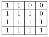
Figure 8 Pattern of bits in memory
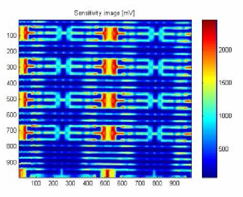
Figure 9 Laser scan of unpowered memory
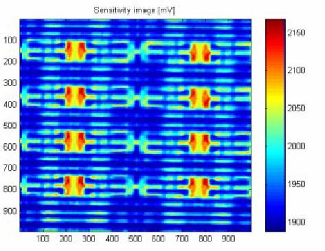
Figure 10 Laser scan of powered-up memory
Similarly, one can use electromagnetic probing techniques to read out a chip’s memory. We built a miniature inductor by wrapping several hundred turns of fine wire around the tip of a microprobe needle. A current injected into this coil will create a magnetic field, and the needle will concentrate the field lines. We obtained the current from a camera, by connecting the coil where the flashbulb should have been. The test probe was then placed a few microns over the surface of the target processor. The magnetic field creates an eddy current in the chip, and we sensed this in order to build a map of the chip (Figure 11).
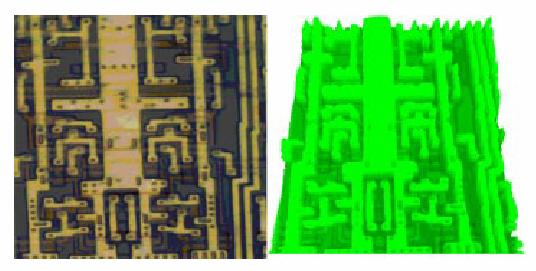
Figure 11 A map built using eddy current and a picture of the same area
We experimented to see whether this fault induction technique could also be used for non-destructive readout. With the same sensor we used to scan the chip, we created a small perturbation on a memory cell. The intensity of the current necessary to recover the initial value of the polarization point was noticeably different between the zero state and the one state. The significance of electromagnetic probing is that optical defences alone are not enough; although it is helpful to give a smartcard chip an opaque passivation layer, it is not sufficient. A continuous metal layer would be preferable - though even this would not block attacks based on the use of infrared lasers through the rear of the chip, or the use of X-rays.
We tested our attack on several static random access memories from different silicon manufacturers, and a few flash memories. We always managed to extract data by one method or another..
This confirms the basic hypothesis of the G3Card project – that more attention should be paid to design techniques such as the use of failure-evident logic with built-in alarm propagation.
If valuable data are present in the clear in memory for just one clock cycle in a location that an attacker can deduce, and the state can be frozen (whether physically, using low temperature, or by some other means such as stopping the clock), then it is likely to be possible for an attacker to read this data out using optical or electromagnetic probing techniques. The investment in skills and equipment required to carry out such attacks is significantly lower than that needed for full invasive attacks. Hardware countermeasures will be necessary for any processors required to resist capable hardware attacks.
contents | 1-overview | 2-background | 3-results summary | 4-results details | 5-deliverables | 6-dissemination | 7-conclusions