ARM project
University of Cambridge, Department of Engineering
Academic year 2003-2004
Easter Term 2004
Project leader: Frank
Stajano
Demonstrators: Dan Gordon, Paul Roberts, Panit Watcharawitch,
Andrew West, Ford Wong.
This project is based on the ECAD
and Architecture workshops designed and lectured by Dr Simon Moore at the
Computer Laboratory of the University of Cambridge. Simon's
cooperation has been invaluable and is very gratefully acknowledged.
ARM project home ||
Tasks (weeks): 1 |
2 |
3 |
4 ||
Feedback (weeks):
1 |
2 |
3 |
4
Introduction |
Timetable |
Weekly mini-reports |
Final report |
Marking |
Bonus track |
Departmental warnings |
Useful online references
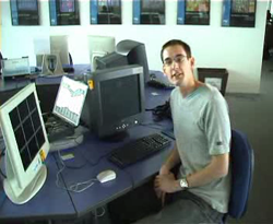
This is everyone.

For posterity: Andy Wild (round of applause) was the only student
who completed this year's bonus track. Click on his nose to see a very
amateurish video (26 MB mpg) of his brilliant achievement.
Introduction
This 4-week project sits at the boundary between hardware and
software. You will be designing hardware circuits and programming a
RISC processor. More specifically, you will build circuits by
programming an Altera FPGA in Verilog (a hardware description
language), and you will connect those circuits to an ARM 7 processor
that you will program in ARM assembly language.
The goal of the project is to build a mouse interface for the ARM
and write a rudimentary device driver allowing the ARM to read out the
absolute 2D position of the mouse.
Timetable
This project runs in the Intel Lab (room SW11, second floor)
at the Computer Laboratory, William Gates
Building on the West Cambridge site. Follow the links for directions;
this is not on the main Engineering site.
Repeat the following pattern for 4 weeks, starting Monday 2004-05-10.
| 2h slot | Mon | Tue | Wed | Thu | Fri | Sat | Sun
|
|---|
| 09:00-11:00 | Mandatory | | | | | |
|
| 11:00-13:00 | | | | Mandatory | | |
|
| lunch
|
| 14:00-16:00 | Mandatory | | | | | |
|
| 16:00-18:00 | Mandatory | | | | | |
|
"Mandatory" means it's a timetabled session for this project. You have
to be there at those times or you will be penalized at the rate of 1
mark per hour missed. I will use some of this time to introduce you to
Verilog and ARM assembler. You will use the rest to program the
devices yourself. During these sessions you will each have access to
an individual workstation with the appropriately licensed software
tools, and you will be issued one teaching board each. Demonstrators
will be available to provide guidance and to help you using the tools
(though not to solve the assignments).
On top of the mandatory timetabled slots, you are expected to spend
about 12 more hours per week on your own on this project. You are
welcome to go to the Intel lab at any time during the opening hours of
the building and use the available facilities when it best suits
you. At those unsupervised times, however, only 6 workstations will be
equipped with teaching boards; the others will have just the software
tools.
Remember that your work for each week is assessed by a demonstrator
on the Thursday of that week, so you have no extra time to clean
things up afterwards.
Weekly mini-reports
In each of the four weeks of the project there is an assigned task
which requires you to program the FPGA, the processor or both. These
four subtasks build on each other.
- Electronic Dice in Verilog (easy)
- String sort in ARM assembler (hard)
- Mouse interface in Verilog (easy)
- Reading the mouse from the ARM (hard)
By the last session of every week you must submit a
mini-report; this includes giving a live demonstration of your
running hardware to one of the demonstrators. The mini-report is much
shorter than the usual "interim reports" of most other projects and
contains practically no prose. It consists of your commented
ARM/Verilog code plus brief answers to a couple of questions on that
week's task. You must submit your mini-report by the last timetabled
session of each week (Thursdays 11:00-13:00). This is a serious
deadline that nobody should miss: the penalty for late
demos/mini-reports is 3 marks per weekday (Mon-Fri), which
means you'd waste at least 6 marks since there is no session on
Fri. It is of course acceptable to submit a mini-report
ahead of time at some earlier session, although you don't get any
extra marks for this.
To submit a mini-report you must
collect three ticks in order, all before that week's deadline:
- Complete the program code (Verilog and/or ARM as appropriate)
required for that week's subtask, ensuring that it is properly
formatted and commented. Follow the format of the supplied template
(Verilog or assembly language).
- Put answers to any questions in comments at the end of your code.
Ensure that you add the subtask's title and your name in a comment at
the top of the code. This set of source code files is your
mini-report.
- Show a running demonstration of your work to a demonstrator to
have it assessed. If the demonstrators points out any flaws, you are
allowed (but not obliged) to fix and resubmit, so long as it's done by
the deadline. Having witnessed your (last) demo, whether your circuit
works or not, the demonstrator will give you Tick #1.
- Email your mini-report as a file attachment to me (fms27 at cam),
with a subject line of "ARM project submission, week N", with N in the
range 1-4 as appropriate. (For some odd reason, it is apparently
very hard for people to write the subject line as requested. However,
if you manage to get it right first time on ALL of your submissions
for this project, I'll give you a small prize of two extra marks at
the end. Easy money!) If your mini-report consists of more than
one file, attach them all to the same mail message. Do not zip, tar,
gzip etc: just send the raw source code (.s or .v). When I receive
your correctly submitted mail, I'll give you
Tick #2.
- Hand in to any demonstrator your anonymous weekly feedback form
and, separately of course, a printed version of your mini-report with
its completed cover sheet. This gets you Tick #3.
All these steps must be completed before the end of the
corresponding Thursday session.
Final report
You must also prepare a final report of not more than 7
pages. It is strongly preferred that you compose it using Latex
and the Springer
LNCS style (use the llncs.cls class found in llncs2e.zip). If
you are new to Latex, here is an example file (Latex source and pdf output) and the style sheet to use. Do
not modify the style sheet. If you use any other method than
Latex, it is your responsibility to make sure that the layout
(margins, font sizes, words per page and so on) exactly matches that
of the LNCS style.
The spirit of the report is to explain to your readers what you
gained, in all possible dimensions, from taking part in this
project. This, of course, will be a reflection of how much you put
in. The report should be a critical assessment of the work performed
and the skills acquired, as opposed to a flat chronicle of what was
done. Even when some of the weekly deliverables were poor or
incomplete, the final report can stil get full marks if it shows that
the author learnt something useful from the experience.
Keep the report to a maximum of 7 sides of LNCS or it will be
penalized in the marking. The recommended format, which will help you
produce a well structured report of the correct length, is as follows.
- Introduction. (0.5 pages).
- Weekly tasks. Individual descriptions of the four weekly
tasks, highlighting your "light bulb" moments (useful insights you got
while performing that week's task, or moments when you got over a
major stumbling block) and any significant design decisions you took
(roughly 0.5--1 page per week, total 2--4 pages).
- Challenges and lessons learned. A commented list of the
most interesting problems you encountered, the way you solved them,
the most useful techniques you adopted to identify and fix bugs in
your Verilog and ARM code, and the general lessons you learned from
your experience with this project. (1--2 pages).
- Conclusions. (0.5 pages).
- Appendix: your weekly mini-reports and their cover sheets (only
the first three, since the last one will not have been returned to you
by the time you submit the final report).
- Complete the last of your supplied cover sheets and prepend it to
the report.
To submit the report:
- Email me (fms27 at cam) a PDF version of the final report as a
file attachment, with a subject line of "ARM project submission, final
report". Do not zip, tar, gzip etc: just send the raw PDF.
- Hand in a printed version of the final report, with your
first three mini-reports as an appendix, to the Teaching Office.
Both of these must be received by 17:00 on Friday 4th June 2004
(last day of week 4 of the project, but not a timetabled
session). This is the most serious deadline of the project: the
department will grant no extensions to it.
Marking
Each weekly mini-report is worth up to 15 marks, for a subtotal of 60
marks. The criteria that will be used for assessment are the
following, most important first.
- Demonstrating a live working solution
- Clearly commenting and formatting the code
- Demonstrating good programming style
- Writing correct code
- Correctly answering the questions
The final report is worth up to 20 marks and will be assessed on the
following criteria.
- Giving a logical and complete account of what was done
- Demonstrating a grasp of the core ideas and skills acquired during the project
- Clarity of ideas
- Clarity of language (readability and correctness of your English prose)
The total for the whole project is therefore 80 marks.
Note that this is not a team project and all work must be
carried out individually.
Bonus Track
The time it takes people to complete the standard tasks varies
greatly. For those of you who can complete the standard tasks in much
less time than allocated, a bonus track is available. Note in passing
that completing a weekly task as soon as possible doesn't usually
yield the highest marks. It is advisable to complete the 4 tasks of
the standard track with elegance and style, particularly with respect
to a legible and well structured source code, before devoting time to
the bonus track.
The main deliverable for the bonus track is a tic-tac-toe (aka
noughts and crosses) game, using the mouse as input and the VGA
monitor as output. The display output and the strategy of the computer
player can be extremely rudimentary: it is ok to use red and green
rectangles (and no grid) instead of the noughts and crosses, and even
to let the computer play entirely at random. Use your own taste.
Unlike what happens with the standard tasks, there will be no
handholding. You will have to find out by yourself how to drive the
monitor (with care so that you don't blow it up) and all the design
choices will be your own, including whether to do everything in the
FPGA or whether to use the ARM as well.
To qualify for the bonus track you must also complete two auxiliary
deliverables.
- Verilog: implement a 2-second delay line—something behaving
like this delay.sof. You will find useful hints in
Simon Moore's ECAD
Workshop 2. Note, however, that the "delay" module on that page,
unlike the one contained in this .sof file, does not really delay an
entire waveform.
- ARM assembly language: implement the prime number program from ECAD
workshop 4.
Bonus track submission
Do all of the following in order.
- Submit all 4 weekly mini-reports as usual.
- Submit (in the same sense of collecting three ticks, and using a
subject line of "ARM project submission, bonus track",) the source
code for the two auxiliary deliverables. Until you do this, your bonus
track deliverable won't be looked at, let alone marked.
- Submit (again: three ticks, and subject line of "ARM project
submission, bonus track") the source for the main deliverable.
- Write a report about the main bonus deliverable, but not the
auxiliary ones, in at most 2 sides of LNCS A4 and include it as part
of your final report.
Bonus track marking
- The two auxiliary deliverables attract no marks, but are required
as preliminaries.
- The source code and live demo for the main bonus deliverable is
worth up to 15 points and replaces, at your own risk if you submit it,
the lowest-scoring of your first three mini-reports.
- Up to 5 bonus points may be awarded to the 2-page report about the
main bonus deliverable.
- Independently of whether you attempt the bonus track or not, you
will receive two bonus marks if the subject lines of all your
file-attached email submissions are as requested.
- The theoretical maximum score for the project is therefore
87/80. After deduction of any applicable penalties, any scores above
80 will be clipped back to 80.
Departmental warnings
- For non-attendance at timetabled sessions you will lose 1 mark per
hour missed.
- For late submission of interim reports you will lose 3 marks per weekday.
- No extension to the final report deadline of 17:00 on Friday 4
June will be permitted.
- You will have to sign a declaration that you are submitting your own work.
- You will not receive any indication of any marks for your interim
or final reports. Your college may inform you of your final mark after
publication of the final class lists.
- Any applications for allowances for illness must be submitted by
your College Tutor to the Teaching Office as soon as possible. It must
be received by Monday 7 June.
Useful online references
Verilog
ARM assembler
- Peter Cockerell's excellent 1987 book ARM
Assembly Language Programming (HTML and PDF) is a useful
reference to keep around while writing code, particularly chapter 3, The
Instruction Set.
- Concise summaries can also be found in Simon Moore's Computer
Design (PDF) course notes, in lectures 3 and 4.
- I can't put a link to it from here, but the ARM developer suite
comes with a library of "Online books" about the tools and the ARM
processor itself. You can access this documentation from the Start
menu: the shortcut is in the same menu from which you launch Code
Warrior.
ARM/Altera teaching board
- The home
page and FAQ
for Simon Moore's ECAD and Architecture workshops at the Computer
Laboratory on which this project is based.
- Documentation
for the board, from an extensive list of memos
about the Altera/ARM hardware.
Related lecture course material