| Computer Laboratory ECAD and Architecture Practical Classes |
Computer Laboratory > Teaching > Course material 2008–09 > All courses > ECAD Labs > Tutorials > SOPC Builder
This tutorial takes you through the steps needed to create the SOPC Builder component used in the second lab exercise. For more detailed information on SOPC Builder or the Avalon Memory-Mapped Interface Specification, see the following documents: Note that this tutorial assumes the custom components required for the project have already been created. For those of you who are interested in creating your own components, details of the different Avalon signals can be found in the Avalon Memory-Mapped Interface Specification. You will need to download and un-zip game_of_life_shell.zip in order to follow this tutorial.
Warning: SOPC Builder uses the Quartus home directory for storing some temporary files whilst it generates
the system. It will not work on the PWF machines since it does not have permission to do this.
Starting SOPC BuilderOpen up SOPC Builder by selecting Tools | SOPC Builder from within Quartus. You will be prompted to specify a system name, give it the name game_of_life. Select Verilog as the target language, and click OK. At the top of the window you will see a section marked Clock Settings. There will be a single clock listed here, with a speed of 50MHz. Double click on the speed and change it to 25MHz. The window should now look like this: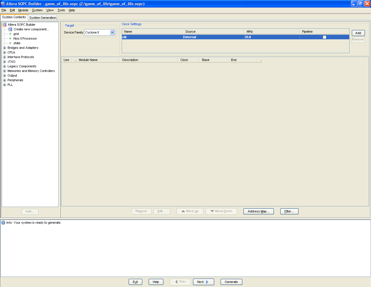
Adding componentsThe next stage is to add the set of components required for the system. Available components are shown in the frame to the left of the window. To add a component, either double-click on it, or select it and click "Add". Add the following components to the system, with the required settings where appropriate:
Note: to change the name of a component, right-click on the module name, and select Rename. Type in the new name, then press Enter. You should now have a system looking like the one below. 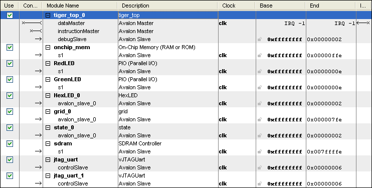
Connecting the modulesYou will notice at the bottom of the screen several error messages informing you that certain components must be connected in order to continue. You connect the components up, hover your cursor over the Connections column in the table. You will notice a grid appear consisting of several wires with white circles where they overlap. A white circle indicates they are not joined, a black one indicates they are connected at that point. Connect both the dataMaster and instructionMaster of the CPU to the onchip_mem and sdram components. Also connect the dataMaster to the cpu debugSlave and also to all other components.The dataMaster IRQ port should be connected to the debugSlave. This should be given an interrupt value of 0. The IRQ column is the right-most column of the table. This should leave the system looking like this: 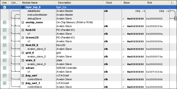
Assigning addressesYou will now notice several other errors have appeared at the bottom of the screen. This is because the current addresses that have been assigned to each component overlap. Each component is mapped onto a different area of the memory, and you can then access the component by reading / writing to these addresses as if you were accessing memory, even though, for example, you may actually be writing data to the 7-segment displays. The Tiger processor contains a cache, which is not ideal for when you wish to write to external peripherals since the data may not be written straight away, and instead cached to "improve" performance. The cache has thus been altered so that any addresses with "1" in the MSB will bypass the cache, as if they were declared "volatile" in C. Therefore, if you decide to expand the system at a later date, perhaps by adding an interface to the LCD module on the board, ensure you assign an address with the MSB set.
To assign the base address for a component, simply double-click on the address, type in the required one and press Enter. Assign
the following addresses to each component:
It is important that you assign the addresses given above, otherwise they will not match with the ones mentioned on the lab sheets. The system should now look like this: 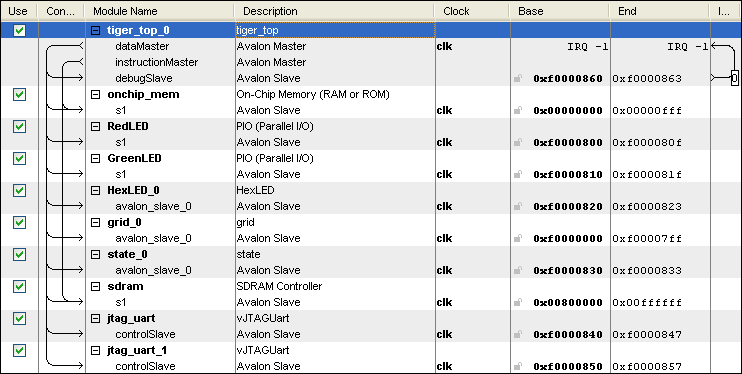
Generating the systemThe final stage is to generate the system and then instantiate the module that is created. Generation causes several Verilog files to be created for each component of the system. It includes a top-level module with the same name as the one given when you first started SOPC Builder, and you instantiate this in the usual way. First, generate these files by clicking Generate at the bottom of the screen. Once SOPC Builder reports back that "System generation was successful" you can now close SOPC Builder and return to Quartus. Add the file game_of_life.v to the project as per usual, and then open this up. Find the module declaration for game_of_life (hint: it may be quicker to search for that term, rather than scrolling through the file!). You will notice several ports in this module. This is the signature of the module that you must now instantiate in the project. To instantiate the module, copy the following code into life.v.
    game_of_life gol(
	.clk(CLOCK_25),
	.reset_n(1'b1),
	.out_port_from_the_GreenLED(LEDG[8:0]),
	.out_port_from_the_RedLED(LEDR[17:0]),
	.HEX0_from_the_HexLED_0(HEX0),
	.HEX1_from_the_HexLED_0(HEX1),
	.HEX2_from_the_HexLED_0(HEX2),
	.HEX3_from_the_HexLED_0(HEX3),
	.HEX4_from_the_HexLED_0(HEX4),
	.HEX5_from_the_HexLED_0(HEX5),
	.HEX6_from_the_HexLED_0(HEX6),
	.HEX7_from_the_HexLED_0(HEX7),
	.address_a_to_the_grid_0(rdaddr),
	.clock_a_to_the_grid_0(video_clock),
	.data_a_to_the_grid_0(8'hXX),
	.q_a_from_the_grid_0(data_out),
	.wren_a_to_the_grid_0(1'b0),
	.mouse_button_to_the_state_0(button_press),
        .next_state_to_the_state_0(!KEY[0]),
        .x_to_the_state_0(cursor_x),
        .y_to_the_state_0(cursor_y),
        .zs_addr_from_the_sdram(DRAM_ADDR),
        .zs_ba_from_the_sdram({DRAM_BA_1, DRAM_BA_0}),
        .zs_cas_n_from_the_sdram(DRAM_CAS_N),
        .zs_cke_from_the_sdram(DRAM_CKE),
        .zs_cs_n_from_the_sdram(DRAM_CS_N),
        .zs_dq_to_and_from_the_sdram(DRAM_DQ),
        .zs_dqm_from_the_sdram({DRAM_UDQM, DRAM_LDQM}),
        .zs_ras_n_from_the_sdram(DRAM_RAS_N),
        .zs_we_n_from_the_sdram(DRAM_WE_N)
	);
You should now be able to compile the project successfully.
Note: due to clock skew on the DE2 board, you cannot simply use the same clock for the SDRAM that is used for the rest of the project. The SDRAM clock should lead the CPU clock by 3 nanoseconds. This is accomplished using a phase-locked-loop like the one created in the first Lab. This has already been set up for this project, however, if you wish to use the SDRAM in your own projects, you may wish to consult the "tut_DE2_sdram_verilog.pdf" tutorial on the DE2 CD for more details.
Note that this will take some time, and so it is advisable to set up incremental compilation first. You will still need to run
analysis & synthesis first, but this is alot quicker than a full compile.
|