| |
Megafunctions - what are they?
|
A megafunction is a pre-built module that performs a commonly required function. This prevent the developer having to write these
modules themselves, hence saving a lot of development time. Altera ship several megafunctions with Quartus covering a range of tasks
such as a FIFO buffer, arithmetic units - add, multiply, divide etc. , several DSP modules, and a lot more besides.
|
Adding a megafunction to a project
|
The DE2 board provides 2 clocks, a 50MHz and 27MHz clock. It also has a connector enabling you to add an external clock source. For this
lab, we will be using the 27MHz clock. However, we are using the
VGA port, which requires a clock frequency of 108 MHz (the bit clock).
One of the megafunctions is a PLL (Phase-Locked-Loop) module that takes an input clock at a certain frequency and produces an output
at another. Before you are able to run the current project, you must first add one of these modules to it.
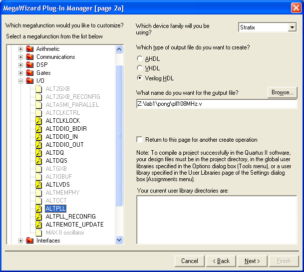
Begin by selecting Tools | MegaWizard Plug-In Manager from the menu, and when prompted, select
Create a new custom megafunction variation On the next screen, there is a tree view on the left hand side showing the
various megafunctions available.
On the right hand side, ensure that Cyclone II is the device family selected, and Verilog HDL is the output language.
Open up the node marked I/O and select ALTPLL in the list that is produced.
Finally, give the file the name pll108MHz.v, ensuring it is saved in the working directory for your project. Click Next
|
|
|
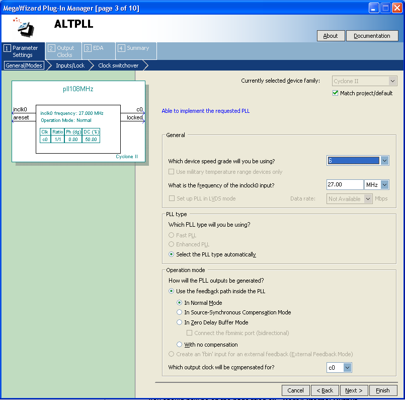
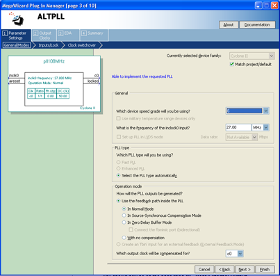
You should now be on page 3 of 10 of the wizard. On this page, set the Device speed grade to 6 and set the
frequency of the inclock0 input to 27.00 MHz. Leave the other settings as default, and click Next.
Since we are interested only in changing the frequency of the clock signal, we do not require the other features this megafunction
provides, such as an asynchronous reset input, thus, un-tick all check boxes on page 4 of the wizard. This should leave 2 wires shown
on the diagram at the top left, inclk0 and c0. Click Next until you reach page 6.
|
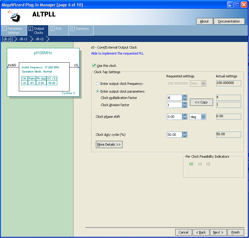
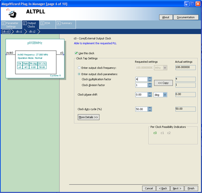
You should now be on the page titled c0 - Core/External Output Clock. This page allows you to specify parameters for the
output clock of this module. Select Enter output clock parameters and enter the following numbers in the respective boxes:
Multiplication factor: 4
Division factor 1
This should give the number 108 in the output clock frequency box under the Actual settings heading.
Click Finish to move to page 10 of the wizard, which displays a list of the files that will be created. Click Finish again
to create the megafunction.
Finally, we need to add the new function to the project and integrate it into the top level module. To do this, firstly select
Project | Add/Remove Files in Project and as before, click on the button with "..." and select the megafunction file
pll108MHz.v, click OK then click Add to add it to the list of files in the project. Click OK to return
to Quartus.
Open up the pong.v file as follows: in the project window, click on the files tab, look under Device Design Files and
double-click on pong.v. Find the comment that says:
// TODO: convert CLOCK_27 to required clock speed
and insert the following line instead:
pll108MHz pll(.inclk0(CLOCK_27), .c0(video_clock));
This instantiates the Megafunction module that has just been created. The module definition can be found in the file pll108MHz.v
|
|
You should now be able to compile the project and upload it to the DE2 board as follows:
Select Processing | Start Compilation to compile the project (alternatively, press ctrl + L). If asked to save
pong.v before continuing, click Yes. During compilation, there will almost certainly be warnings appearing at the
bottom of the screen, but these should not be a problem. Warnings which mention unused pins or reduced registers due to optimisation are generally OK.
Warnings which mention truncated values, for example "truncated value with size 32 to match size of target (11)" may be ok, for example,
the code counter <= counter + 1; will raise this warning type, but can be ignored. If your design compiles but
doesn't work as you expect, check these warnings as it may well be you forgot to add a size when declaring a register, ending up
with 1 bit rather than 10, say.
Next, ensure your DE2 board is connected to the power supply and turn it on. You should see a pre-programmed sequence running on the
board. Connect your monitor up to the VGA output, and connect the board to the computer via. the USB cable. Make sure the cable is
plugged into the USB socket labelled BLASTER on the board. Select Tools | Programmer, and at the top make sure
USB-Blaster [USB-0] appears next to Hardware Setup. If not, click on Hardware Setup, double-click
USB-Blaster [USB-0] in the list box then click Close.
In the list box, there should be pong.sof listed here. This is the file that you are going to upload to the FPGA. If it is
not there, double-click on the first line and choose the file from the dialog box that opens. Select the box under
Program / Configure, then click Start to program the board. After a few seconds you should see on your monitor an
image like the one to the right. You now have the DE2 Board running :-)
|

|
 | Your final task is to read through the renderer module and edit the code to display a checkered pattern like the one on the
left. Remember you are designing hardware, so use of complex operators like modulus is expensive whereas accessing particular bits and
performing simple logic operations is cheap.
|
As an optional extra, modify the rendering code further to display
the colour spectrum, like in the image to the right.
Note: a common problem is that the calculation
used is too complex to be completed in a one clock cycle, i.e. the
circuit doesn't meet timing. This usually manifests itself as
unwanted colour bands. Check the timing information post synthesis.
|
 |
|