
ECAD and Architecture Practical Classes
Creating a Simple System on Chip
Select File | Save. Call your project hello_world and click Save.
Adding Components
Double-clicking a component on the Component Library tab adds it to the System Contents tab. Most components allow you to set up various parameters prior to being added; unless stated, these should remain unchanged. You need to add the following components:
- Clock Source
- One is provided in the default project. A clock source component receives (often external) clock and reset signals to be used within the system. Double click the Clock Source component in the System Contents tab to open its properties. Set the Clock frequency to 100000000 Hz (100MHz, the next page explains why) and click Finish.
- NIOS II Processor
- Look under Embedded Processors. Set Reset vector memory and Exception vector memory to Absolute. These give the absolute addresses to which the program counter (PC) is set when either a reset or exception event occurs. Click Finish.
- JTAG UART
- Look under Interface Protocols | Serial. This provides buffered character streaming between the SoC and the host PC. This allows interaction with the system via a NIOS II terminal.
- Interval Timer
- Look under Peripherals | Microcontroller Peripherals. This is used to allow accurate measurement of time by providing periodic interrupts.
- SDRAM Controller
- Look under Memories and Memory Controllers | External Memory Interfaces | SDRAM Interfaces . The tPad has two SDRAM chips, external to the FPGA; these are logically combined into a single interface (wires), available via the Quartus pin assignments. The controller provides an interface which export from the Qsys project for connection to the SDRAM pins in the top-level SystemVerilog file of the Quartus project. Right-click on the SDRAM controller and select Rename. Type sdram_0 and press Enter.
- PIO (Parallel I/O)s
- Look under Peripherals | Microcontroller Peripherals. A PIO is essentially a memory-mapped register of specified width. A connected device with a compatible interface (number of wires) may read or write this register, according to the type of PIO. We will need two: one will allow output to 8 of the red LEDs; another will allow input from 3 of the buttons (we could alternatively have a single-bit PIO for each button). Set the width and direction appropriately for each PIO.
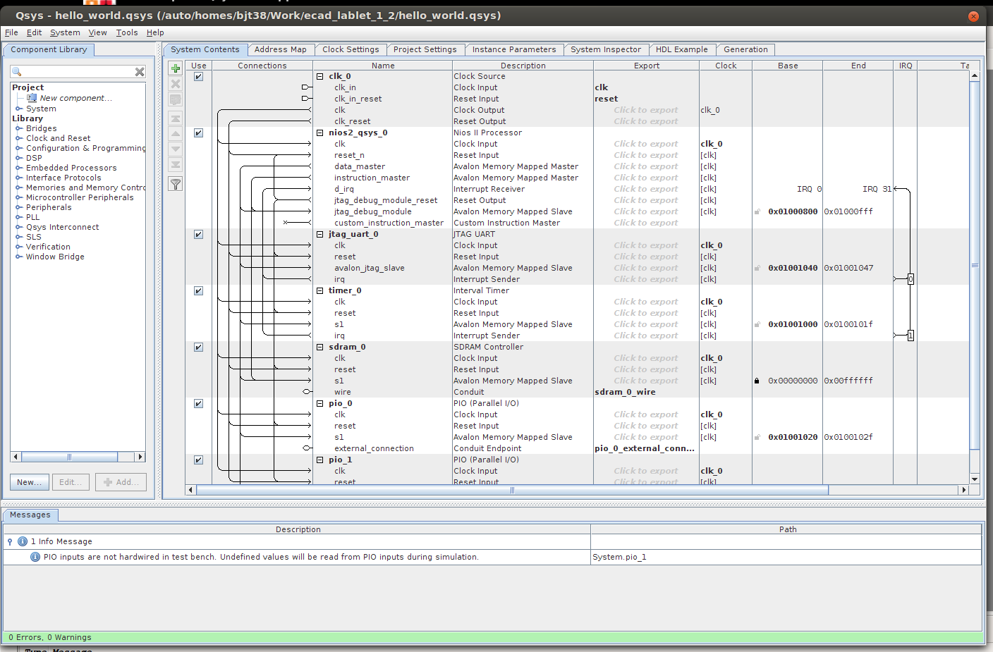
At this point your project should resemble that shown below, but without any connections between components yet. Ignore the errors and warnings for now.
Connecting Components
In the main panel, look in the Connections column on the System Contents tab. The interface of each component is displayed graphically as a set of lines; each line corresponds to a sub-interface (wires).
Let's connect the Clock Output interface of the system clock clk_0.clk to the Clock Input interface of the NIOS II processor, nios2_qsys_0.clk: click on clk_0.clk and follow the bold, grey line to its intersection with nios2_qsys_0.clk. Where compatible interfaces' lines cross, a circle appears: an empty circle indicates the interfaces are not connected; clicking the circle toggles the state. Click the circle to make a connection. The line between clk0.clk and nios2_qsys_0.clk now turns black, indicating that there is a connection.
In a similar manner to the example above, make the following connections between the Qsys components:
- Clocks
- Connect all Clock Input interfaces (except clk_0.clk_in) to the Clock Output interface of the system clock, clk_0.clk.
- Resets
- Connect all Reset Input interfaces (except clk_0.clk_in_reset) to the Reset Output interfaces of the system clock, clk_0.clk_reset and the NIOS II JTAG debug module nios2_qsys_0.jtag_debug_module_reset. Note that this can be done automatically by selecting System | Create Global Reset Network. At this point all of the erros in the Messages pane should disappear.
- Bus Interconnect
- Connect all Avalon Memory Mapped Slave interfaces to the Avalon Memory Mapped Master interface of the NIOS II processor, nios2_qsys_0.data_master. Also connect nios2_qsys_0.instruction_master to sdram_0.s1. Some new errors will appear - ignore these for now.
Interrupt interfaces are hidden by default. Right click anywhere in the System Contents and select Filter | All Interfaces. In the IRQ column, connect all Interrupt Sender interfaces to the NIOS II Interrupt Receiver interface, nios2_qsys_0.d_irq.
Look in the Export column. This shows the interfaces (wires) that are exposed to the Verilog module that instantiates this Qsys SoC. Double clicking in "click to export" exports the corresponding interface (press the Enter key to confirm). Ensure that clk_0.clk_in and clk_0.clk_in_reset are exported. Also export all three Conduit (Endpoint) interfaces.
Bus Configuration
In the main panel, look in the Base and End columns on the System Contents tab. These show the memory-mapped address ranges for each memory-mapped slave in your system. You need to partition the address space to ensure that these ranges do not overlap.
Ensure the Base address of the SDRAM is set to 0x0000_0000 (corresponding to the NIOS II reset vector) and click the padlock to lock it there. Now click System | Assign Base Addresses to perform the partition automatically. There should now be no errors or warnings. If there are, you have not set up your system correctly. Compare it carefully to the screenshot above.
Generation
Click the Generation tab and then click Generate. This produces Verilog modules represented by your system, including the necessary interconnect logic to make the connections you specified. Generation should report no errors or warnings. After generation has finished click Close.