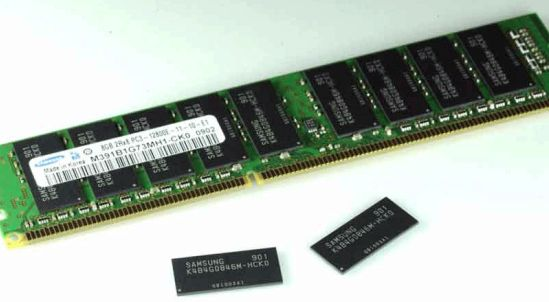
DRAMs for use in PCs are mounted on SIMMS or DIMMS. But for embedded applications, they are typically just soldered to the main PCB. Normally one DRAM chip (or pair of chips to make D=32) is shared over many sub-systems in, say, a mobile phone.
SoC DRAM compatibility might be a generation behind workstation DRAM: e.g. using DDR3 instead of DDR4 Also, the most recent SoCs embed some DRAM on the main die or flip-chip/die-stack the DRAM directly on top of the SoC die in the same package (multi-chip module --- MCM).
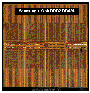
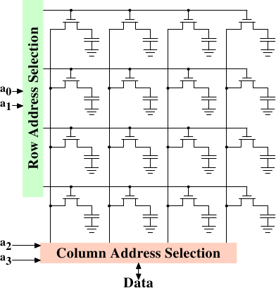
Modern DRAM chip with 8 internal memory banks.
 |  |
These are the pin connections of a typical DIMM from 2010:
|
|
Our DIMM example has a 200 MHz clock and hence 400 MT/s. This is low performance by today's standards: 64 bits times 400 MHz gives 25.6 Gb/s peak (4 GB/sec).
The capacity is a 1 Gbyte DIMM made of 8 chips. The latest (Jan 2018) DDR4 memories operate at 4332 MT/sec. Each transfer caries a word the width of the DRAM data bus (e.g. 16 bits) and transfers are performed on both edges of a clock. This clock would be at 2.166 GHz. But that is the burst transfer rate. To manage a burst, DRAM timings of 19-21-21 are used, which is the number of clock cycles to send the row address, the column address and for writeback, respectively.
In the worst case, if the DRAM is currently `open' on the wrong row, 61 clock cycles will be needed to change to the new location. Roughly the same number of clock cycles again will be used in pipeline stages through the various memory hierarchy levels of the controlling device.
| 14: (C) 2008-18, DJ Greaves, University of Cambridge, Computer Laboratory. |