|
|
|||||
| Computer Laboratory Workshop Five |
||
| Computer Laboratory > Course material 2005-06 > Hardware Practical Classes > Workshop Five |
Workshop Five - nMOS and CMOS invertersIntroductionIn this workshop you will investigate FET transistor characteristics by building and measuring nMOS and CMOS inverters (see lecture 8 for background information). Components
Step 1: Characterise nMOS InvertersTask 1: Build the nMOS inverter circuit shown below on the breadboard. Make sure you properly identify which of the leads is the source, drain and gate before inserting it into the breadboard. Connect the potentiometer and resistor as shown. To characterize this inverter, you will need to measure how the output voltage varies with the input voltage. 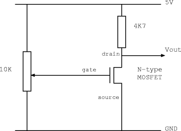 Task 2: Connect one of the oscilloscope probes to the drain of the transistor and the other to the gate. Vary the gate voltage from 0 to 5V in steps of 0.2V using the potentiometer. At each step, measure the voltage at the drain. Plot a graph of drain vs gate voltage showing the transistor switching. Comment on the point where x=y. Task 3: Find the points of negative slope (-45°) on your transfer curve. It is these points that define the boundary between valid logic levels and the indeterminate region. Using this information, find the range of valid input voltages for a logic 0 and the valid input voltages for a logic 1. Answer questions 1 and 2. Tutorial on Noise MarginsIf you look at the electrical characteristics section of the data sheet for a 74HC series IC, you will find that the manufacturer guarantees that the gate will recognize any input voltage above 2.4V as a logic 1 and will recognize any input voltage below 2.1V as a valid logic 0 input. On the output side of the gate, the minimum guaranteed logic 1 output voltage is given as close to VCC (in our case 5V). The maximum logic 0 voltage is around 0.1V Notice that the minimum output high voltage (4.9V) is 2.5V higher that the minimum voltage required for an input high on a following gate (2.4V). A difference of 2V also exists between the maximum logic 0 output voltage and the maximum logic 0 input voltage. These differences are referred to as noise margins. They ensure that a small noise transient on a connecting wire cannot change the state of the next gate. It is normal to quote the smaller of the two values, in this case our inverter has a noise margin of 2V. 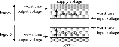
Step 2: Characterise a CMOS inverterRepeat the above with the following CMOS inverter and questions 3 to 5. WARNING: ensure you connect the source and drains of the transistors as shown since if you get them the wrong way around the transistors will conduct and burn out. As a safety precaution you could put a small resistor between the power supply and your inverter to limit current, but remove this resistor before taking your final measurements. 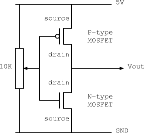 Step 3: Characterising a ring of two invertersTask: Connect two CMOS inverters together as shown in the circuit below. Connect the outputs from the two inverters to LEDs. CAREFULLY and BRIEFLY (in case you've got the circuit wrong!) short to ground the inputs of each inverter in turn. Record the behaviour and answer questions 6 to 8. 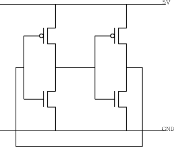 Step 4: Characterising a ring of three invertersTask: Add another inverter to your ring so that your circuit has three inverters as shown below. Also add a capacitive load to the output of each inverter (0.1uF should do). Look at the output from two of the inverters on the oscilloscope. Answer questions 9 and 10. 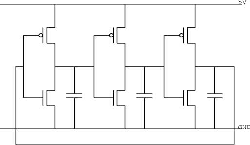 Optional Bounus StepMeasure the switching current of a CMOS inverter. AssessmentTicking criteria: Write up your experimental data and answer the following questions. Once your work has met the Common Ticking Criteria (see Introduction), get your work ticked by an assessor. Remember that you need to hand in this assessed exercise as part of your portfolio of work (see the Head of Department's notice). Questions
1. What is the noise margin of the nMOS gate if it was connected to
another similar gate? |
![]()