| Parameter | Value | Unit |
| Drawn Gate Length | 0.08 | µm |
| Metal Layers | 6 to 9 | layers |
| Max Gate Density | 400K | gates/mm² |
| Track Width | 0.25 | µm |
| Track Spacing | 0.25 | µm |
| Tracking Capacitance | 1 | fF/mm |
| Core Supply Voltage | 0.9 to 1.4 | V |
| FO4 Delay | 51 | ps |
| Leakage current | nA/gate |

The mainstream VLSI technology in the period 2004-2008 was 90 nm.
Parameters from a 90 nanometer standard cell library:
|  |
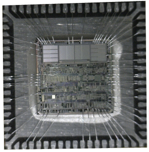
Typical processor core: 200k gates + 4 RAMs: one square millimeter.
Typical SoC chip area is 50-100 mm² → 20-40 million gates.
Actual gate and transistor counts are higher owing to custom blocks (RAMs mainly).
Now the industry is using 35-45 nanometer.
» Moore's Law » Transistor Count