The Excalibur board is based around an Altera EPXA1 IC, which
contains a reasonably sized FPGA, and an ARM9 processor with various
peripherals. To help transfer data between the ARM and the FPGA, there
is an AHB data bus, and 16kB of dual ported RAM. On the demo board
itself there is Ethernet, two serial ports (one of which must be
implemented in the FPGA), SDRAM and Flash memory.
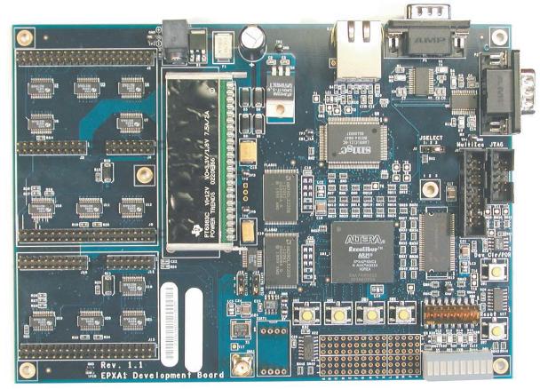
The board also has two expansion headers which special I/O boards
connect to, providing a safe way to connect other devices to the
IC. We will be using these in later practicals.
|
|
|
|
|
PART 1 - Starting Quartus and making a new Project
|
| |
|
|
|
|
|
|
|
|
 |
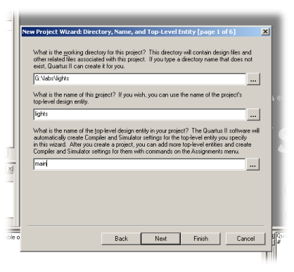
First create a new directory for the first part of this workshop in
your filespace for the project, perhaps called lab1\lights (N.B. don't put spaces in the directory names since this will cause difficulties later on when you run the tcl script). Into this,
download the file main.v and
excalibur_pins.tcl. Sometimes (for
some reason best known to itself), Internet Explorer adds "(1)" to the
end of file names when you download them - make sure you don't save
it with this. The files are, respectively, a Verilog hardware
description file, and a TCL script to set up your project.
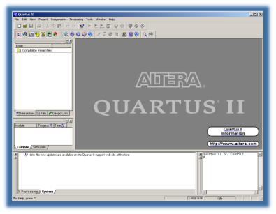
You should now open the Quartus II program from the Start
menu (it's in PWF Programs | Teaching Packages | Computer
Laboratory and called Quartus II 4.2. Once loaded, it
should look like the screen on the left. In the bottom left corner
there is the messages window, with the status window just above it on the left.
If you can't see them, turn them on from the View | Utility Windows
menu.
|
Now, select File | New Project Wizard..., click Next
and enter the information as shown in the screenshot on the right
(with your directory specified). The project will be called 'lights',
but the top level entity must be called 'main' since the TCL script assumes
it. Click Next.
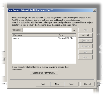
|
On Page 2, you must specify the files that are in your
project. Click the "Add..." button and select
the main.v file that was downloaded previously. Page 3 allows you to choose the
type of device to compile for; the demo boards use Excalibur parts, so
choose EXCALIBUR_ARM from the drop down list, and make sure
that 'Specific device selected in 'Available devices' list' is checked. Choose
EPXA1F484C1 as the device, and leave the other three settings
as 'Any'. The next page allows you to choose which tools are to be used by Quartus. At the moment
we'll just be using the standard Quartus tools, so all tool checkboxes should be
unchecked. You can then click Finish and the project will be
created. Open the verilog description file (main.v) with File |
Open...
|
Now the project has been created, the TCL script
needs to be executed so that it can set up the pin assignments. Use
Tools | TCL Scripts... and click on excalibur_pins under
Project and then click Run. The script will take a few
seconds to run and status will appear in the window at the
bottom.
The project is now completely
set up, and you should be able to click the Start Compilation ( ) button, or the menu option under
Processing. The Messages and Status window should show how the
compilation is doing, and when it is finished a window will be displayed,
hopefully saying compilation was successful. There will almost certainly be
warnings, but these aren't fatal. ) button, or the menu option under
Processing. The Messages and Status window should show how the
compilation is doing, and when it is finished a window will be displayed,
hopefully saying compilation was successful. There will almost certainly be
warnings, but these aren't fatal.
Now the project has compiled, it can be uploaded to the Excalibur
demo board. Go to Tools | Programmer. Next to the Hardware
setup button check to make sure it says "ByteBlaster [LPT1]". If
not, click on the Hardware setup button and then Add
Hardware, select ByteBlasterMV or ByteBlaster II and press
OK. Back in the hardware setup window, select the
ByteBlaster [LPT1] from the "Currently selected hardware" list,
and then click Close. Once you have the ByteBlaster installed,
click the auto detect button. This will detect all devices on the
JTAG chain - there should be 2 of them (if not, change the jumper on
the EPXA1 board marked JSELECT to the 2-3 position and try
again). Right-click on the one marked EPXA1 and choose Change
File (you can also use the toolbar button or double-click where it
says "1. <none>"). Select main.sof, and tick the
'Program/Configure' box. To upload, click the Start button on
the top of the toolbar that appeared on the left of the work area.
Tip: sometimes
the EPXA1 device number is not recognised by the current version of
Quartus. Usually the EPXA1 device is the first one on the device
chain, so right click on it, Change Device and then select
EXCALIBUR_ARM fron the first list and EPXA1 from the
second list. Then repeat the above instructions from Change
File.
Tip: To allow
the programer configuration to be saved you need to ensure that both
devices on the JTAG chain are defined. The second JTAG device is the
ARM processor and can be configured by right clicking on it, Change
Device and select EMBEDDED_PROCESSOR from the first list
and EPXA-ARM922 from the second list. Then you can save the
JTAG configuration (ctrl-S).
After this, the LED bar graph on the demo board should light up each
LED in turn. You can also use the PC to simulate the logic, and a\
brief walkthough of using Quartus' simulator is provided below.
First a waveform file needs to be created. This is a simple way to
specify the input signals through a graphical interface. These signals provide
input to the FPGA in the simulation.
- Click File | New... and select Other Files | Vector
Waveform File, or click the button (
 ), to
bring up the vector waveform editor. ), to
bring up the vector waveform editor.
- Right-click on the left-hand pane of the window labelled
Waveform1.vwf and click Insert Node or Bus....
- In this new window, click Node Finder. This window allows you to
select parts of your design to look at and change at simulation time.
- Make sure Named is set to '*'
- and that Filter is Pins: all.
- Click List. The list on the left should now show all the pins that
the project uses (CLK, LEDS, LEDS[0], etc.).
- Select CLK and LEDS and click the right-arrow button to add them to the right-hand list.
- Click OK, and OK again, and two lines should now have been
added to the waveform window.
- Click on CLK to select the waveform for the clock input.
- Click the clock button
 on the left. on the left.
- Set Period to 25 Mhz and click OK. This will replace the CLK waveform with a clock like that on the Excalibur board.
- Choose Edit | End Time... and choose 1 ms. You can also set
up the state of inputs for brief periods of time by highlighting the area you
want, and selecting one of the buttons on the left. There isn't any need for
that here though.
- Save the waveform file to main.vwf.
- To tell Quartus to simulate with the vector file, you
have to use Tools | Simulator Tool
- At the top, make sure simulation mode is set to
Functional (this is not as accurate, but is far quicker than
Timing simulation).
- For the simulation input, choose main.vwf as the settings
file.
- Make sure that Simulation runs until the Vector Stimuli
have been used is selected.
- Make sure all the other simulation options are turned off.
- The last thing you need to do is generate the netlist for the simulation by choosing
Processing | Generate Fuctional Simulation Netlist (or by using the button at the top of the Simulator Tool window).
|  |
Now everything is set up, you can just choose Processing | Start
Simulation or click the button ( )
and the simulation should begin (if it asks, there is no need to save
the CDF file). When the simulation is done, click the Report button at the bottom of the Simulator Tool window, or choose Processing | Simulation Report. You can use the magnifying glass to zoom out, and
clicking on the '+' button by LEDS will expand the bus into its
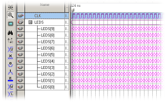
component data lines. You will find that there is no useful output.
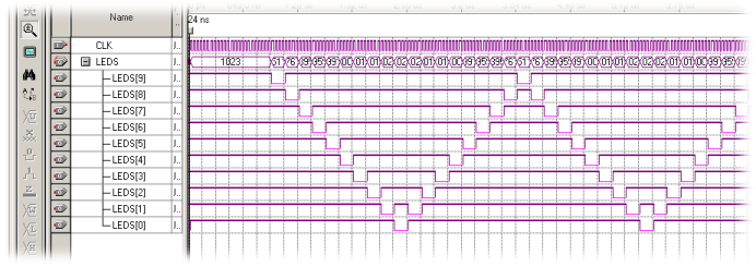
Why? How can you make a minor adjustment to your Verilog code in
order that a useful simulation can take place? We would like to see a
result like the one below showing each LED changing (output going low)
in turn. )
and the simulation should begin (if it asks, there is no need to save
the CDF file). When the simulation is done, click the Report button at the bottom of the Simulator Tool window, or choose Processing | Simulation Report. You can use the magnifying glass to zoom out, and
clicking on the '+' button by LEDS will expand the bus into its
component data lines. You will find that there is no useful output.
Why? How can you make a minor adjustment to your Verilog code in
order that a useful simulation can take place? We would like to see a
result like the one below showing each LED changing (output going low)
in turn.
Tip: it is often useful to probe
internal state to aid debugging. So, for example, go back to your
waveform stimulus file (main.vwf) click Insert Node or
Bus... and Node Finder as before, but this time set
Filter to 'Registers: pre-synthesis', click List and add
'counter'. Now resimulate.
|
|
|
|
|
PART 2 - Electronic Door Lock
|
| |
|
|
|
|
|
|
|
|
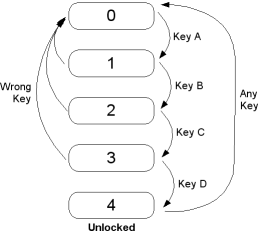 |
The idea of this part of the practical is to create a simple 4
digit electronic door lock in the FPGA. The four switches on the demo
board (SW2/3/4/5) will have to be pressed in the correct order before
an LED on the LED bar graph lights to show that the FPGA is
unlocked. The illustration to the left shows a simple state
diagram. However, when the lock is implemented in the FPGA, it is
recommended that more states are used. When the correct button is
pressed, a state should be entered, and when it is released, the state
should change again. This allows the combination to consist of the
same button pressed two or more times.
In addition to a state machine, you will have to make a module to
debounce the switches.
Download main.v and excalibur_pins.tcl into a new
directory for the project. excalibur_pins.tcl is the same file as last
time, but the new main.v contains the outline of a Verilog file
that should be the door lock. Set up a project in the new
directory, as was detailed above, and then make the following
additions to main.v:
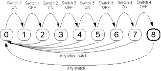
Add the switch debouncing module to main.v (see ECAD lecture 4).
Set up the bottom 4 LEDs on the bar graph (LEDS[3:0]) to
indicate the state in binary. Remember that the LEDs turn on when the
output is 0, not 1. Set the remaining 6 LEDs (LEDS[9:4]) to light up
if state is 8 (unlocked).
In the case statement, fill in an action for each
state. The code here will dictate which sequence of buttons opens the
lock. For example, if the lock's code was ADCB, in state 0, if A was
pressed (and no other switches), state 1 should be entered. In state
1, if A was released, state 2 should be entered, but if any other key
was pressed, the state should be set to 0. The unlocked state, 8,
should return to state 0 if any key is pressed.
|
Questions
- In part 1: what did you have to change in order to obtain useful
simulation results and why?
- In part 2: why did the switches need to be debounced and what
would happen if they were not debounced?
- In part 2: how long does your debouncer wait before deciding
whether the switch was pressed or released?
Ticking criteria
Ticking procedure
- Show your work to one of the demonstrators (on screen or
paper). They will award you with a tick if the work is up to
standard.
- Print out your final work and add it to your portfolio to be
submitted as instructed in the Head of Department notice.
|