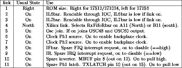
The port controller revision 2 PCB has a number of configuration links. Table 10 lists them, and the usual settings. Many of the links cause spare signals to be pulled up or down, these may be useful for experiments or modifications. The Xilinx link enables the pin out of a 3064 to differ from the 3042 in the position of the RxFifoRbar signal, which requires a fast path output. 3042 designs may only use the B11 (south) setting of this link, 3064s may use either. The Osc Join link enables use of a single oscillator module for the CPU and memory clocks.
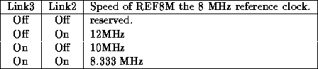
Links 2 and 3 are provided for the Port Controller to discover the speed of its 8 MHz reference clock. They provide a 2 bit number from which the mapping is described in table 11.