Pcb and PALs


Next: Appendix - code
Up: DAN Processor Node: The
Previous: BOS software
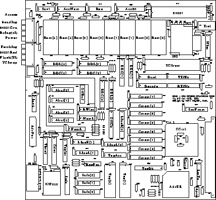
Figure 4: MDH-9 PCB chip locations
The silk screen printed layer of the MDH-9 PCB is shown in figure
4. This has had the chip names added to ease identification.
The CPU is held on a separate daughter card. This allows the PQFP
device to effectively be socketed, and also terminates the unused
coprocessor bus lines.
Most of the logic on the MDH-9 is provided by PALs or Xilinx FPGAs.
The two xilinx devices are a 3064 which acts as the cache controller,
and a 3020 which serves as the address multiplexor and comparator.
Much functionality has had to be moved into devices with faster I/O
timings, so the controller xilinx is supported by PALs and fast TTL
logic. The PALs used on the card are:
- Acc68 22V10
- Controls access to the 68901. Generates the data strobe
and either CSb or IACK, and controls the asynchronous access. This PAL
also combines the remove wait signals to feed the fast wait logic.
- Accmem22V10-10
- Times access to ROM and local SRAM. Also
generates the SRAM write pulses.
- Cdec 22V10-10
- Cache Decode PAL. Enables the cache
databus buffers, decodes the address and miss information
to give the access mode and
the cache set required. Also generates the update signal for the info system.
- Decode 22V10-10
- Decodes the address lines for all local devices
(ie with address bit A31 clear). The ROM and RAM chip selects are also
generated.
- Dual 22V10
- Under control of the cache control xilinx this
PAL produces the address lines for fetching the VCI from the dual port ram.
- Info 22V10-10
- Manages reading and updating the cache information
- the dirty and LRU bits.
- Misc 16R8-7
- Divides down the crystal to produce the CPU
clocks and the 4MHz reference clock for the 68901.
- OffCk 22V10-10
- Generates the read and write enables for the cache
RAMS and checks the offset for crossing a line boundary.
- Res 16V8
- The reset PAL generates the reset pulse in responce to
any one of the four reset sources requesting. The reset reason is
output, and may be read via the 68901.
- TagAcc 16V8-10
- Generates the read and write enables for the cache
tag rams and the address latches.
- Time2 22V10-10
- Detects the need for the CPU to wait and starts the
fast logic. Also generates the drive signals for the bi-colour access
LED and the data bus buffers.
Next: Appendix - code
Up: DAN Processor Node: The
Previous: BOS software
Mark Hayter