ARM project: Week 1
Electronic dice in Verilog
ARM project home |
Tasks (weeks): 1 |
2 |
3 |
4
Setting up the project
First create a new directory for the first part of this workshop in
your filespace for the project, perhaps called w1/tlights/. Into this,
download the files:
- tlights.v
- Verilog source file. For your reference, this circuit simulates
a set of traffic lights that cycle through a sequence of Red,
Red+Amber, Green, Amber, as illustrated in the first example
of Simon Moore's
ECAD lecture notes.
- tlights.qsf
- Quartus settings file, including the mapping between
pins and signal names.
Sometimes (for some reason
best known to itself), Internet Explorer adds "(1)" to the end of file
names when you download them—make sure you don't save them with
this.
Editing the verilog source
You should now open the Quartus II program from
the Start menu (it's in
and called on the PWF).
Start by creating new project using . At each step enter these settings:
| Page 1 |
Working Directory:
U:/arm/w1/tlights
(your directory containing tlights.v
and tlight.qsf)
Name of project:
tlights
Top level entity:
tlights
|
Screenshot |
| Page 2, 3 |
No Changes
|
|
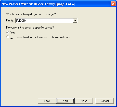
| Page 4 |
Family:
Flex10K
Target Specific Device:
Yes
|
Screenshot |
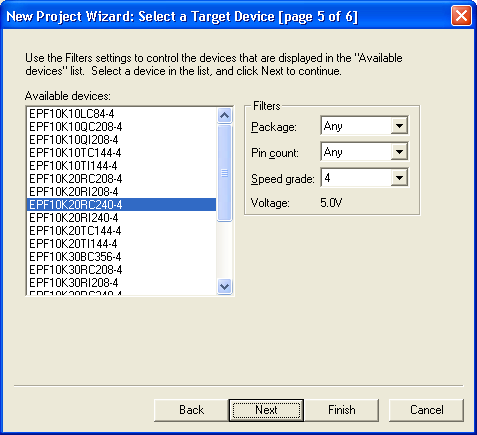
| Page 5 |
Speed Grade:
4 (you must choose this first)
Device:
EPF10K20RC240-4
|
Screenshot |
To open the project later use the dialogue box.
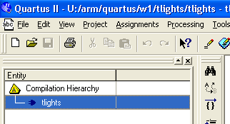
Notice that a hierarchy window has opened containing an
entry named tlights - this represents the Verilog source file. Double
click it to open the file in an editor.
Pin and device assignments and the .qsf file
The file tlights.qsf contains the pin and device assignments. It would be instructive for you to check these yourself by following this proceedure:
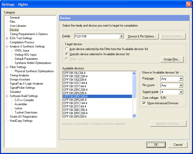
-
The type of chip designated to a design can be viewed using the
dialog. This should be correct
already, but it is as well to check. We will be using an
EPF10K20RC240-4. The box should look like this:
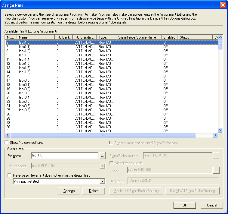
-
Next, while we're here, take a look at the
dialogue box. Again,
this should already be correct but note that each of the ports of the
top-level module has been assigned a pin number, to correspond with
the pins which are actually connected to things on the board. The
dialogue box will look like this:
If there are no pins named led, check that the title bar of the Quartus II window indicates the right project name—it should be the same as the path to
tlights.qsf, without the .qsf
extension—
for example U:/arm/w1/tlights/tlights
. If it isn't, you may have forgotten to
download the .qsf settings file. Close the
dialogue box and start again.
Alternatively click on the Assignment Editor button
 followed by the Pin button
 located in the upper right of the window.
When you assign pins in the future, you'll need to make sure you've
assigned the right sort of device beforehand.
These assignments are saved in the tlights.qsf file. You may
wish to open it and have a look. For a large number of pin assignments, it is much
easier to edit this file than to use the dialogue box.
Compiling the project
We can now compile the project. Start the compiler by choosing
, or clicking on the
shortcut button, which looks like this: 
The software should now compile the design. During compilation a
number of warning are shown at the bottom of the screen in the
Messages Window. These complain about the fact that we have made pin
assignments. You can ignore this.
In compiling, it will generate many files, of which some are
useful, and some aren't! At present we are interested in tlights.sof, which is the object file used to
program the FLEX chip.
Introduction to the hardware
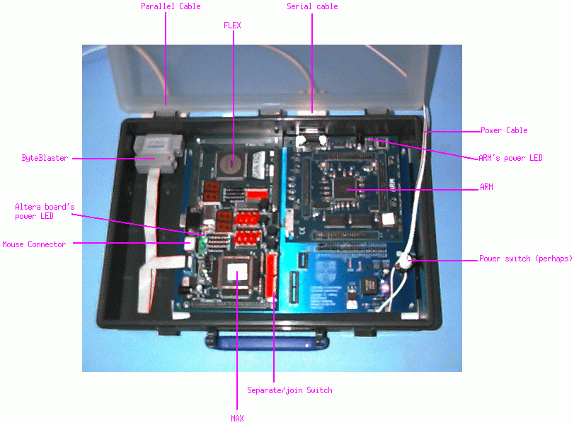
In the case there are three boards. The one on the left is the
Altera board, which we are using for this week's task; the one on the
right is the ARM board, and the board underneath links them together
and provides a power supply.
The Altera board has two Programmable Logic Devices; the rearmost
one is the one we shall be using, and is called the FLEX; its
programmable element is an SRAM, meaning it must be reprogrammed
whenever it is first turned on.
The frontmost device is the much less powerful MAX. Its
programmable element is an EEPROM, meaning it retains its
configuration even when powered off. It has been programmed to
protect the ARM when both boards are being used, since it would
otherwise be possible to short out the ARM's pins. All signals
between the FLEX and the ARM pass first through a resistor, and then
the MAX. If the MAX detects that a short has occurred, it turns off
all its outputs and displays "Er" (for error) in the LED segments.
There is also a switch to separate the two boards: it is the very
first switch, on the right of the board. It should be switched up
for this lab, to separate the boards. Check this is the case.
The board is programmed via an interface called JTAG. This is very
flexible, but we shall only be using it to program the FLEX chip.
Check that the jumpers are set correctly for this: from the back, they
should be to the left, left, right and right.
The data for the JTAG interface comes down the ribbon cable going
to the connector on the back of the box. This short bit of cable is
called the ByteBlaster, and it converts parallel data
from the computer into the JTAG format. Of course, both the parallel
cable and the power cable have to be connected to your computer before
anything will work!
Programming the Altera FLEX chip
At last we can program the chip. This is done as follows:
-
Open the Programmer, by choosing
-
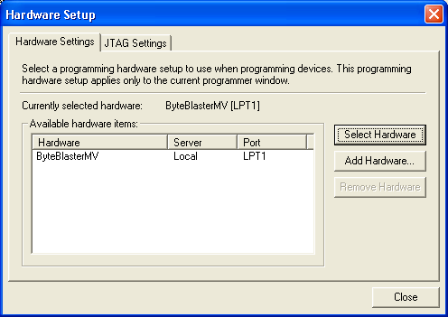
The first time you use the programmer it must be told to use the
ByteBlaster hardware. If the hardware field does not read
ByteBlaster MV [LTP1] open the Hardware Settings dialog
then click Add Hardware. Add a ByteBlasterMV on LPT1
then make sure it is selected. It should
finish looking like this:
-
Close the Hardware Setup dialog.
-
The file tlights.sof should be listed in the Programmer window. If not, use the Add File button to add the file (it can be found in your project directory).
-
Enable the Program/Configure option for tlights.sof.
-
Click on Start. This should download the .sof file to the board, instantiating the circuit, and the LEDs should display a traffic light sequence.
Having done this, play around a little on your own. Ensure that you
can connect up the pushbuttons and displays in any way you desire, and
that you know how to display numerical values on the LEDs. Build a
counter, maybe a backwards counter, whatever. Above all,
enjoy the fun!—that's the most effective way to learn at a
deep level.
Using the simulator
Next, we'll investigate the use of the simulator, and some of the
difficulties associated with using it.
You must now create the waveforms that are the stimulus for your circuit. These waveforms are saved in waveform vector files with the extension .wvf.
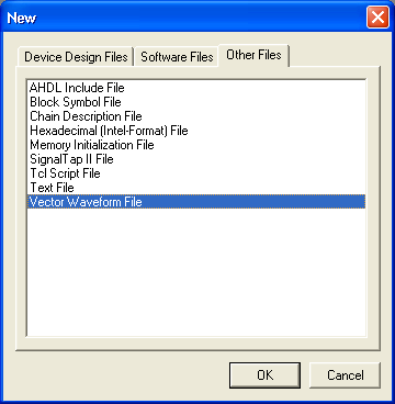
Create a new waveform vector file using menu
option. "Vector Waveform File" is located under the Other Files tab like this:
-
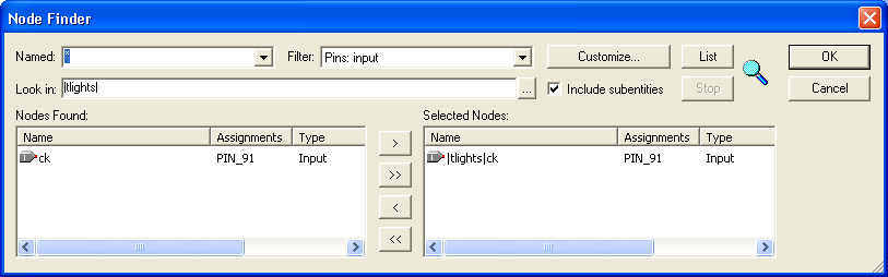
Add your chips clock input pin to the waveform. To do this use
and click Node Finder. Click on "List" to
show the nodes available for adding to your waveform. This generates
a large list of nodes; so, narrow the search by choosing Pins:
Input as a filter and clicking "List" again. The Named:
box allows you to search by name ("*" matches anything).
Select the ck pin and choose to add it to your wvf using the
> button. The dialogue box should now look like this:
-
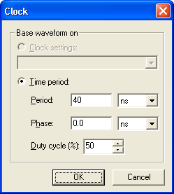
Each waveform is assigned a logic zero by default so you must connect a
clock signal to your ck pin.
Select the ck signal by clicking on it (it will be highlighted blue) then use the
Assign Clock button
 to open the Clock dialog. Enter a period of 40ns, duty cycle 50% like this:
-
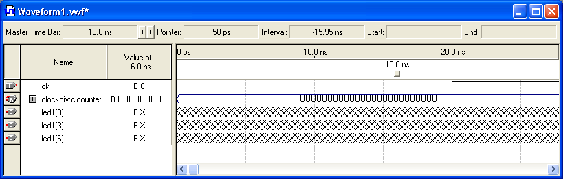
Continue by using the Node Finder dialog to add the nodes
clockdiv:c|counter,
led1[0],
led1[3], and
led1[6].
The completed waveforms should look like this:
-
Save this file as tlights.wvf and close the waveform window.
The creation of stimulus for your circuit is now complete.
Before simulation can be performed your project must be prepared for simulation. Make sure there are no compilation error messages then use
to prepare your circuit.
Open the Simulator Tool dialog at
.
We want to run a Functional simulation (see the Quartus II help system for a description of this and the alternative Timing simulation) so choose Simulation mode
as "Functional". Enter tlight.vwf as the simulation input and end the simulation at 1 us. Deactivate the option Automatically add pins... then click Start to save settings and begin the simulation.
When the simulation is complete use the Report button to view the Simulation Waveforms report. You will probably need to use the zoom tool  to see more of the waveforms (Tip: right mouse button zooms out). Right-click on the counter waveform, choose "Properties", and change the display radix of the counter to "Hexadecimal".
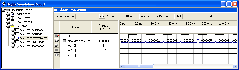
You will notice the counter operates correctly but the LED outputs are stuck at 1 in the simulation. Why is that? How can you modify the Verilog so that you can exercise the traffic light sequencer?
Question 1
W1-Q1: Why were the LEDs stuck at 1 in the simulation, and what was
your fix?
Having done that, note that the supplied code is not synchronous: it
derives a 'slow clock' signal and (yecchhh) uses it to clock the
flip-flops of the traffic lights state machine. You know this is
wrong. Fix it.
Question 2
W1-Q2: What did you do to turn the traffic lights into a
synchronous circuit?
Electronic Dice
Now we'll take the Verilog one stage further. In this project, you
should end up with dual working electronic dice; however, it is up to
you exactly what form the system will take.
You should aim for a working project that produces two random
numbers, each between 1 and 6, each time a button is pressed. You may
want to blank the display while the button is being pressed, but that
is not necessary. The usual approach to this is to implement a counter
which is clocked faster than the eye can see. While the button is
pressed, the counter counts, and when the button is released, the
current value of the counter is frozen, and appears on the display. As
long as the counter is clocked at a sufficiently high speed, the
effect should be that of randomness.
Starting a new project
Before we begin, we need to set up the FLEX chip. Download the file dice.qsf - this contains many useful settings, like pin assignements. Make a new directory called "w1/dice/", and place this
file inside.
To start a new project, load the Quartus II
software, and select the menu option . Enter the same settings found in the tlights project but use the name "dice" for the project and top level entity.
Your new project initially contains no files. Open the dialog box and select "Verilog HDL File". You should be presented with an empty editor window. Use and edit this template for any Verilog file you write. Enter the following skeleton for the top level module (the inputs and outputs mirror the definitions in the .qsf file):
module dice(ck, button1, led1, led0);

    input ck;
    input button1;
    output [7:0] led1, led0;

endmodule
You will also need the hextoleds.v file. Download this into
your project directory. It provides a module with the following signature:
module hexToLeds(byte, led1, led0);
where 'byte' is an 8-bit input, and led1 and led0 are the bottom 7
bits of the outputs to the digit displays.
The project code
Undoubtedly, you will want to write a module that counts from 1 to
6. It should take two inputs: the clock, and an input telling it
whether to advance or not. Combining these into one input is generally
not safe practice: it is not a good idea to gate a clock, as it
causes problems with propagation. The module should output a binary
value on a three or four-bit data bus. (As a module designer, why
would you choose one over the other? Can you see the merits of both
choices?)
You can output this counter to bits 0-2 or 0-3 of the hextoleds. You can assign the remaining bits of the
hextoleds input to zero.
Save all your code in a file called "dice.v" in the new w1/dice/ directory. Your top-level module must
have the same name as the filename (without the ".v"). Compile,
download, and run the program.
Useful debugging tips
To obtain additional debugging from the synthesis tool turn on the
Design Assistant by opening . Under "Design Assistant" select the Run Design Assistant during compilation option.
Remember that this Verilog compiler is rather lax: just because
something compiled, it doesn't mean that it is bug-free. In some cases
you would expect a compiler warning if you do something silly by
mistake (e.g. connecting a bus of the wrong width into a module), but
you probably won't get any. So it pays to be extra careful.
Remember also that the location at which the compilation stops with
an error message may not be the real location of the error. Try
checking for syntax errors in the lines above.
Question 3
W1-Q3: Is there any need to debounce the push button switches in
your design? Why? And can you describe a design in which the opposite
answer would be more appropriate?
Weekly mini-report
Submit your mini-report before the end of the last timetabled session
of this week according to the usual rules.
You must supply a full source listing for the electronic dice, but
not for the traffic lights, hextoleds or anything else.
Be sure to include the answers to the three questions in a comment
at the end of your source.
Please don't leave submission to the last moment: expect queues for
the demonstrators' attention during the last hour. If you haven't
submitted by the end of the Thursday session, your next chance is on
Monday, but with a penalty of 3 marks per weekday (i.e. 6
marks). Worth avoiding.
Once you've finished
How good a random-number generator do you think this is?
Hint: week 2 is more complex so it may be a good idea to get
familiar with next week's task and tools ahead of time.