|
|
|||||
| Computer Laboratory Workshop Four |
||
| Computer Laboratory > Course material 2004-05 > 1A Hardware Workshops > Workshop Four |
Workshop Four - Framestore for an LED ArrayIntroductionThis experiment is designed to show the operation of a framestore and introduce the use of a Static Random Access Memory (SRAM). The design uses the SRAM as a framestore for two 5x7 LED arrays. The LED display is made up from individual LEDs which are connected in a grid. Connecting a row (through a current limiting resistor) to the power rail and a column to ground lights the LED where they cross. This means that although each LED can be lit individually, an arbitrary pattern cannot be displayed merely by applying constant voltages to the row and column inputs. Instead, the array must be scanned, preferably at a rate at which the display does not appear to flicker. In this experiment, the pattern to be display is to be read from an SRAM. 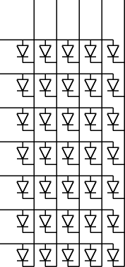 Components
Step 1 - Make the LED matrix light upTask: Use the 74HC193 IC to produce a 4-bit counter. Make sure that the unused input pins are tied appropriately. Use this 4 bit value as the column address for scanning the LED array. Tie the row inputs to logic 1 (the supply voltage). Step 2 - Connect the SRAM to the LED matrixTask: Use the same 4-bit value as the address for the SRAM and connect the data output from the SRAM to the rows of the array, making sure that the CS, OE and WR pins are tied appropriately to fix the chip in read mode. Unused address pins should be connected to ground. 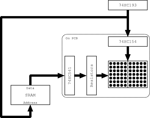 Your circuit should now display the random contents for SRAM on the array. Turn your power supply on and off several times to see if the pattern changes. Step 3 - Add an SRAM write circuitTask 1: The next part of this experiment is to add some
circuitry to allow values to be write into the SRAM. The complete
circuit should look something like this: 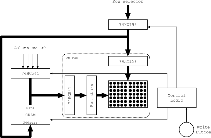 Connect the output of the 74HC541 octal buffer to the data bus, and use seven toggle switches as its input. Now connect the column selector (binary coded rotary switch) to the input of the binary counter. When complete, you should be able to write the data from the toggle switches into the SRAM at the address supplied by the column selector. This should only happen when a write button is pressed. Task 2: Design the control circuit using a 74HC74 and a 74HC00 chip. The behaviour is as follows: as the write button (use the debounced switch) is pressed, the value from the rotary switch should be loaded into the binary counter. The value from the row switches should be driven onto the data bus, and the write pin on the SRAM chip should be pulsed. Inputs to the control circuit will be the clock and the write button. It needs to produce three outputs: an enable signal for the octal buffer, a write pulse for the SRAM and a load signal for the counter. Start by producing a timing diagram showing the clock oscillating and the switch being pressed. Fill in what you want the outputs to do as the switch is pressed and goes high. You might like a demonstrator to check before proceeding to the final design. Tips:
Optional Bonus StepImplement a "clear display" button which writes zeros into the SRAM. AssessmentTicking criteria: Write up your experimental data and final design, then answer the following questions. Demonstrate that your circuit works correctly: you should be able to specify a column on the LED array with the column selector and the data pattern for that column with the toggle switches. Pressing the write button should make the pattern permanent. Once your work has met the Common Ticking Criteria (see Introduction), get your work ticked by an assessor. Remember that you need to hand in this assessed exercise as part of your portfolio of work (see the Head of Department's notice). Note: because this workshop is a little tricky, one tick is awarded for completing steps 1 and 2 and question 1, and the other tick for step 3 and question 2. Questions
1. Each LED in the matrix can draw a maximum current of 5mA. What is
the maximum current that the two LED arrays can draw during the
operation of the frame store? |
![]()