⇡ Tutorial for the debug preview of lowRISC
Soc structure updates
Thanks to the continuous development from the RISC-V group at UC Berkeley, there are a lot of structure changes and extra features incorporated in this release.
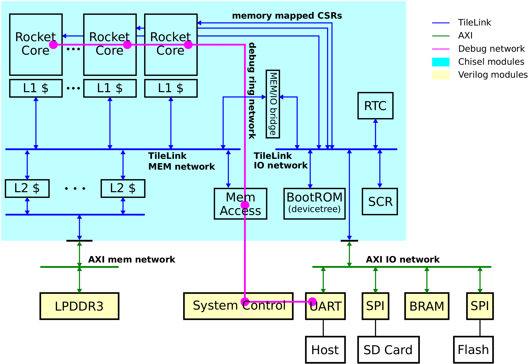
Shared TileLink MEM network for both cached (memory) accesses and uncached (IO) accesses.
In the previous untethered release, cached memory accesses and uncached IO accesses are separated early in the L1 D$, which has the benefit of small on-chip interconnects and less interference to the memory interconnect from IO transactions. However, this leads to troubles when a peripheral, such as a DMA, needs to access the memory (L2 cache). This release follows the choice from the upstream Rocket design that separates uncached IO transactions from cached memory accesses at the coherent TileLink MEM network. As a result, the debug MAM module can access memory as well as all IO space by a single access point to the MEM network.A global memory space regulator: address map
A static data structure is added into the Rocket-chip to regulate the size and the R/W/X permission of all memory sections. It uses a hierarchical map to store all memory sections. For the standalone FPGA demo, the map should look like:
<"io", 0x00000000-0x7fffffff>
<"int", 0x00000000-0x3fffffff>
<"bootrom", 0x00000000-0x00001fff, RX>
<"rtc", 0x00002000-0x00002fff, RW>
<"prci0", 0x00003000-0x00003fff, RW>
<"ext", 0x40000000-0x7fffffff>
<"bram", 0x40000000-0x4000ffff, RWX>
<"flash", 0x41000000-0x40ffffff, RX>
<"uart", 0x42000000-0x42001fff, RW>
<"spi", 0x42002000-0x42003fff, RW>
<"mem", 0x80000000-0xffffffff, RWX>
Note that the base address of each memory section is calculated automatically during the Chisel compilation. For a detail look of the address map, please read the related part in$TOP/src/main/scala/Configs.scala(initialization of the address map) and$TOP/junctions/src/main/scala/addrmap.scala(implementation of the address map).Boot ROM
A boot ROM is added into the SoC, which should always located at the reset address (0x00000000 by default). The current boot ROM has two parts: The first several instructions redirect PC to the on-chip BRAM if it is enabled or to the DDR RAM. The rest of the ROM has a configuration string, which stores a simplified device tree. This configuration string identifies the number and types of processors on chip along with the address map. For the standalone FPGA demo, the configuration string should read as:
platform {
vendor lowRISC;
arch rocket;
};
rtc {
addr 0x2000;
};
ram {
0 {
addr 0x80000000;
size 0x8000000;
};
};
core {
0 {
0 {
isa rv64imafd;
timecmp 0x2008;
ipi 0x3000;
};
};
};
This configuration string is automatically generated bymakeBootROM()in$TOP/src/main/scala/LowRISCChip.scalaNote that not all sections in address map is recorded in the configuration string. We will rectify this soon. With this configuration string in the boot ROM, bootloaders and the Linux kernel are able to probe the SoC structure without external device tree files.