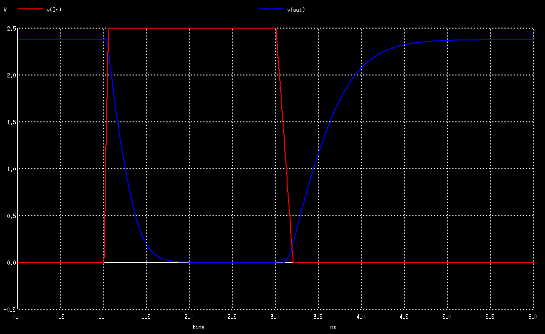
Plot when running from a VCC supply of 2.5 volts. Red is stimulus and blue is output.
Here is a complete demo of simulating a CMOS inverter made from two MOSFETs using hspice.
// spice-cmos-inverter-djg-demo.hsp // Updated 2017 by DJ Greaves // Based on demo by David Harris harrisd@leland.stanford.edu /////////////////////////////////////////// // Set supply voltage//////////////////////////////////////// // Declare global supply nets and connect them to a constant-voltage supply .global Vdd Gnd Vsupply Vdd Gnd DC 'VddVoltage' /////////////////////////////////////////// // Set up the transistor geometry by defining lambda .opt scale=0.35u * Define lambda // This is half the minimum channel length. // Set up some typical MOSFET parameters. //http://www.seas.upenn.edu/~jan/spice/spice.models.html#mosis1.2um .MODEL CMOSN NMOS LEVEL=3 PHI=0.600000 TOX=2.1200E-08 XJ=0.200000U +TPG=1 VTO=0.7860 DELTA=6.9670E-01 LD=1.6470E-07 KP=9.6379E-05 +UO=591.7 THETA=8.1220E-02 RSH=8.5450E+01 GAMMA=0.5863 +NSUB=2.7470E+16 NFS=1.98E+12 VMAX=1.7330E+05 ETA=4.3680E-02 +KAPPA=1.3960E-01 CGDO=4.0241E-10 CGSO=4.0241E-10 +CGBO=3.6144E-10 CJ=3.8541E-04 MJ=1.1854 CJSW=1.3940E-10 +MJSW=0.125195 PB=0.800000 .MODEL CMOSP PMOS LEVEL=3 PHI=0.600000 TOX=2.1200E-08 XJ=0.200000U +TPG=-1 VTO=-0.9056 DELTA=1.5200E+00 LD=2.2000E-08 KP=2.9352E-05 +UO=180.2 THETA=1.2480E-01 RSH=1.0470E+02 GAMMA=0.4863 +NSUB=1.8900E+16 NFS=3.46E+12 VMAX=3.7320E+05 ETA=1.6410E-01 +KAPPA=9.6940E+00 CGDO=5.3752E-11 CGSO=5.3752E-11 +CGBO=3.3650E-10 CJ=4.8447E-04 MJ=0.5027 CJSW=1.6457E-10 +MJSW=0.217168 PB=0.850000
/////////////////////////////////////////////
// Define the inverter, made of two mosfets as usual, using a subcircuit.

.subckt myinv In Out N=8 P=16 // Assumes 5 lambda of diffusion on the source/drain
m1 Out In Gnd Gnd CMOSN l=2 w=N
+ as='5*N' ad='5*N'
+ ps='N+10' pd='N+10'
m2 Out In Vdd Vdd CMOSP l=2 w=P
+ as='5*P' ad='5*P'
+ ps='P+10' pd='P+10'
.ends myinv


//////////////////////////////////////////////
// Top-level simulation netlist
//  One instance of my inverter and a load capacitor
x1 In Out  myinv         // Inverter
C1 Out Gnd 0.1pF         // Load capacitor

//////////////////////////////////////////////
// Stimulus: Create a waveform generator to drive In
// Use a  "Piecewise linear source"  PWL that takes a list of time/voltage pairs.

Vstim In Gnd PWL(0 0 1ns 0   1.05ns 'VddVoltage'   3ns VddVoltage    3.2ns 0)

//////////////////////////////////////////////
// Invoke transient simulation (that itself will first find a steady state)

.tran .01ns 6ns // Set the time step and total duration
.plot TRAN v(In) v(Out)
.end
// To get an X-windows plot, run the following interactive sequence of commands:
// $ ngspice spice-cmos-inverter-djg-demo.hsp
// ngspice 11 -> run
// ngspice 12 -> plot v(In) v(Out)

// end of file
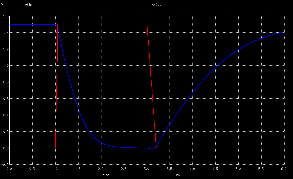
The output load capacitor experiences a fairly typical exponential charge and discharge shape. The shape is not a true 1-exp(-t/CR) curve owing to some non-lineariy in the MOSFETs. But it is pretty close. If the FETs had equal on resistance at the two supply voltages, although the swing of the ouput in the two plots would be different, the delays before they cross the half-supply level would be identical. The difference arises owing to the on resistance being less when the gate voltage is less (i.e. when it is closer to the transistor threshold voltage).
| 7: (C) 2008-18, DJ Greaves, University of Cambridge, Computer Laboratory. |