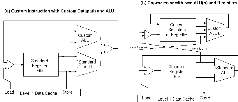
A custom ALU operation implemented in two similar ways: as a custom instruction or as a coprocessor.
Suppose something like the following fragment of code is a dominant consumer of power in a portable embedded mobile device:
  for (int xx=0; xx<1024; xx++)
  {
     unsigned int d = Data[xx];
     int count = 0;
     while (d > 0) { if (d & 1) count ++;   d >>= 1; }
     if (!xx || count > maxcount) { maxcount = count; where = xx; }
  }
This kernel tallies the set bit count in each word: such bit-level operations are inefficient using general-purpose CPU instruction sets.
This is about the smallest possible example for which a hardware accelerator might be worthwhile. Do you think it could be worthwhile?
A dedicated hardware accelerator avoids instruction fetch overhead and is generally more power efficient.
Analysis using Amdahl's law and high-level simulation (SystemC TLM) can establish whether a hardware implementation is worthwhile.
There are several feasible partitions:
The special hardware in all approaches may be manually coded in RTL or compiled using HLS from the original C implementation.
In the first two approaches, both the tally and the conditional update of the maxcount variable might be implemented in the custom ALU, but most of the gain would come from the tally function itself and the detailed design might be different depending on whether custom instruction or coprocessor were used.
The custom instruction operates on data held in the normal CPU register file. The bit tally function alone reads one input word and yields one output word, so it easily fits within the addressing modes provided for normal ALU operations.
Performing the update of both the maxcount and word registers in one custom instruction would require two register file writes and this may not be possible in one clock cycle and hence, if this part of the kernel is placed in the custom datapath we might lean more towards the co-processor approach.
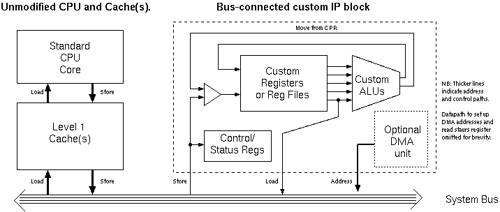
Whether to use the separate, bus-connected IP block depends on whether the processor has something better to do in the meantime and that there is sufficient bus bandwidth for them both to operate. Whether the data is likely to be in or be needed in a given L1 data cache is also an important factor.
The separate IP block may or may not use a DMA controller. Given that the ARM now has a ones-tally instruction in its normal ALU, getting an ARM to move the data into the separate IP block may be a really poor design point.
With increasing available transistor count in the form of dark silicon (ie.\ switched off most of the time) in recent and future VLSI, implementing standard kernels as custom hardware cores is a possible future trend for power conservation. The conservation cores project »Venkatesh~ considered implementing the inner loops of a `mature computations' such as a selection of popular Android applications in silicon on future mobile phones.
| 3: (C) 2008-18, DJ Greaves, University of Cambridge, Computer Laboratory. |