Xilinx interface.


Next: Software
Up: FPC3 Xilinx Xi5Design and
Previous: TXRX Xilinx (Taxi5)
The interface and registers will be very similar to the ``xi3''
design. The basic outline is shown in the Xi5/Xi6 Info sheet. The
``TimeStamp'' generated by the xilinx consists of the status register
in the top 16 bits and the FRC in the low 16 bits. Thus it includes
source and time information.
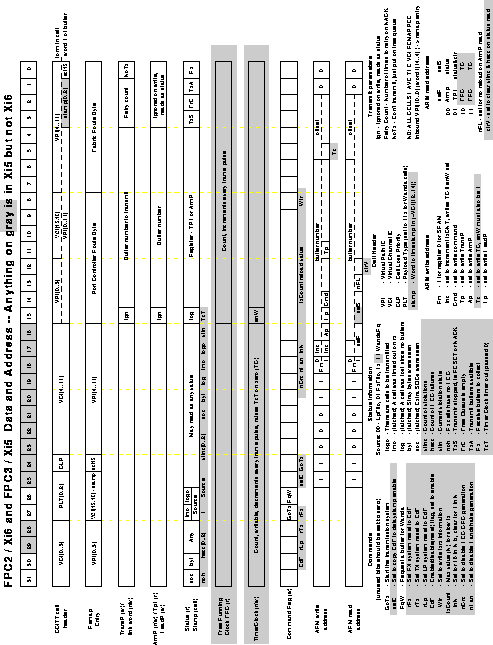
A read operation from a register (Rm set) uses the selR
field to select the register to be read in the low 16 bits, and the
selS to select the status register to be read on the top 16
bits. In addition there are two flag bits. nRL is only used if
ArmP is being read and should be set to prevent automatic reload. clrV is only used if the status register is read, and causes the
violation and HECfail counters to be cleared.
A write to memory may cause the transmit buffer counter to be
incremented by setting the Inc bit in the address. In this case
if the data written has the enW bit set then the top 16 bits of
the data will be written to TC as well as to memory.
In a write to registers address bits are used to select the
register(s) to be written. There is nothing to stop data being written
to several registers in the same operation. Again the Inc bit
may be set to cause the transmit counter to increment. TC will be
written if bit enW is set in the data and either the Tc
bit or the Inc bit is set in the address.
The command register interprets the bit pattern given and peforms zero
or more operations. Bits should be set to enable the operation.
- GoTx. Start the transmission system after a reset or NACK.
It is the responsibility of the software to ensure all the
pointers and links are in a sane state before this command is
issued.
- setD. Set the internal delay-stamp enable flag from EdF. This allows the automatic timestamping of cells based on
their VCIin to be enabled and disabled.
- RqW. Requests a buffer be moved from the free queue to the
recieved queue. This operation will be performed as soon as the
receive system is searching for a new start of cell. Only one
request will be held pending, until the buffer has been unlinked
from the free queue additional requests are ignored. The buffer
will have the TimeStamp written in both words 0 and 1 so software
may detect it by the top VCI bit being set.
- rRx,rTx,rLp. These three bits enable updating of the reset
state of the three fifos. For any enabled lines the EdF
value is copied into the reset register. If the reset register bit
is zero (which it will be after the xilinx is reset) then the fifo
is disabled and reset.
- Wtr. If this bit is set then the TxRx chip parameters are
loaded. The txCount value is used as the reload value for a
down counter which reloads on reaching zero. The counter
decrements at the byte transmit rate. If the inN bit is
clear then data will only be transmitted when the count is zero,
if inN is set transmission is enabled whenever the count <
16. The nHan and nCrc bits replace the links on the
old transmission card, and if set disable handshake and HEC CRC
generation.
The interupts generated by the xilinx are shown in table 3.
The IR and IF lines are edge triggered, so will only generate an
interupt when the status appears. The current value of those signals may
be read via the IOC control register.
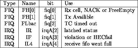
Table 3: Xilinx interrupts
Next: Software
Up: FPC3 Xilinx Xi5Design and
Previous: TXRX Xilinx (Taxi5)
Mark Hayter and Richard Black