The xilinx gate array on the port controller is configured in peripheral mode
(M0=+5V M1=gnd M2=+5V) for easy programming under software control.
There are three status lines which come from the xilinx chip to the
IOC. These are INIT, HDC and RDY/BUSYbar which appear in IOC status
register B![]() as noted in table 5.
as noted in table 5.
In addition to the data there are three control lines which affect the xilinx chip. These control lines are manipulated by the processor through a simple PAL. These lines are the WriteStobe (WRTbar) active low line, a low to high transition on which causes the current value on the data lines to be read in by the chip. The other lines are the reprogram line which can be used to cause an already programmed chip to be wiped, and the reset line which is connected to global reset on the chip. In addition the PAL controls the enable line of a buffer between the IOC data bus lines and the xilinx data lines.
On power on reset or board reset the PAL asserts and holds the reset signal and deasserts all other signals. This ensures there are no board conflicts and prevents the xilinx chip from operating until the software chooses to bring it out of the reset state.
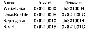
The PAL operations are controlled by the address bus only, appearing in the IOC space at device 1, see table 6, and are activated by a write to the given address. For FPC1 the pal equations may be found in /usr/groups/fairisle/designs/portc/revisions/palrev3.{pld, map}. For FPC2 the pal equations may be found in directory /homes/mdh/portc/fpc2pal.
The first thing that the software does is to being the chip out of reset and wait for the INIT signal to go inactive. This indicates that the xilinx chip has completed its internal clearing operation. (If the chip has currently got a configuration in it then this signal will not have gone active and the chip will be running with the old configuration).
Then the HDC (High During Configuration) signal is tested. This signal is not valid during reset or initialisation phases but otherwise indicates if the chip is ready to receive a configuration. This signal will be high at this point iff there is no configuration in the chip. If this signal is low then the chip must have its current data removed, this is performed by asserting the reprogram line for a short period and waiting for the INIT line to go inactive. The xilinx allows for the HDC pin to become a user I/O pin after configuration but this is not permitted on the port controller. This line has a pull down resistor so can be left unused in the xilinx design.
In either case the chip is now ready to be programmed. This is performed by loading the configuration data bytewise, with the BUSY line being checked to ensure handshaking. Bytes are written using four operations. This is not quite right but it goes something like this:
It should be noted that these operations are extremely sensitive not only to delay but also to potential accesses to the I/O space. For this reason these operations should be performed with interrupts disabled. Once all the data has been written the HDC line should be checked for inactivity to ensure that the chip has accepted the data and assumed the configuration. After configuration strobing the reset line will reset the xilinx device, clearing all the internal flipflops. If this is done the fifos should also be reset using the IOC control line (see table 2).
Once the xilinx has been programmed the WriteData line may be used by the processor to control the xilinx, and the XiRdy line may be used by the xilinx to generate a processor IRQ interrupt. Currently neither of these are used.