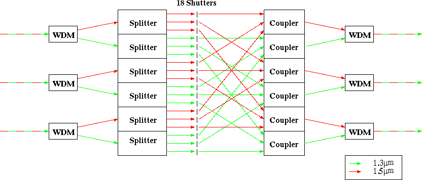
The optical signal from one of these sources is combined with signals from other such sources in order to produce a WDM signal. The combined optical signal is transmitted into the Granta Network were it goes to the optical switch, situated at Engineering. The optical switch is a 3x3 port device capabable of routing 1300nm signals differently from 1550nm signals. It takes each input fibre and first splits it three ways, then each of these three ways is WDM demultiplexed into a total of six fibres.
Each of the six fibres (3 in, 3 out) which connect to the switch are split in the same way, making a total of 36 fibre ends. These fibre ends are interconnected with 18 optical shutters arranged as two 3x3 crossbars, one for each wavelength.
The shutters consist of a 3cm free space optical path with a LCD panel in the middle. More exotic switches will be tried in future projects. The outputs from the switches are routed back to the three sites and wavelength split into separate monocolour channels. Each channel is fitted with an optical to electrical convertor. The serial output from the optical receiver is converted into a 40 bit parallel format by a card containing fast chips. The 40 bit data stream is tested by a card containing an XC4010D FPGA which notes errors and reports them to another ARM PIE microprocessor card over an 8 bit parallel handshook link.