This week concludes the project, so it's time to learn a bit about hardware/software codesign. Your task is to interface and access the mouse from the ARM. You will be writing a small program for the ARM as well as reusing and modifying some of the Verilog you have written for week 3. The work is split into two jobs to help you build up the hardware and software in stages.
Your first job is to interface the ARM to the 7-segment LEDs controlled by the FLEX chip on the Altera board. This will be used in job 2 to display mouse data, but for job 1 you could just display an incrementing number. The FLEX chip has been allocated a chunk of the ARM's address space and so it needs to act like an memory device to allow the ARM to write data to it. In job 2 the FLEX will also allow the ARM to read data from it.
You need to write some Verilog code for the FLEX to latch data written by the ARM, decode the data (using the HexToLEDs module you know and love) and output the hex digits on the LEDs.
To make the FLEX respond to write requests from the ARM, you will need to:
Pin definitions for the FLEX chip are in fullmouse.acf. To get you started with your Verilog, below is some suitable code for the top level module, including the mouse interface and data output bits needed for job 2 (which you can ignore for now) and the tristate buffer for nWAIT mentioned above.
module fullmouse(led1, led0, mdata, mclock, d, a,
    XCLK, nCE2, nOE, nWE, INT4, nWAIT);

    output [7:0] led1, led0; // 8-bit outputs to LEDs
    inout mdata, mclock; // mouse serial interface
    inout [7:0] d; // bidirectional data bus
    input [7:0] a; // address bus
    input XCLK, nCE2, nOE, nWE; // clock and memory bus control
    output INT4; // interrupt 4 line
    inout  nWAIT; // bidirectional memory timing control

    TRI tbuf_for_nWAIT(1, 0, nWAIT); // make nWAIT be "z"
    // TUT: the tristate buffer takes (input, enable, output)

    wire [7:0] data_out = 0; // zero data output to ARM for now
    wire enable_data_out = 0; // don't output data to ARM for now
    TRI tbuf_for_D0(data_out[0], enable_data_out, d[0]);
    TRI tbuf_for_D1(data_out[1], enable_data_out, d[1]);
    TRI tbuf_for_D2(data_out[2], enable_data_out, d[2]);
    TRI tbuf_for_D3(data_out[3], enable_data_out, d[3]);
    TRI tbuf_for_D4(data_out[4], enable_data_out, d[4]);
    TRI tbuf_for_D5(data_out[5], enable_data_out, d[5]);
    TRI tbuf_for_D6(data_out[6], enable_data_out, d[6]);
    TRI tbuf_for_D7(data_out[7], enable_data_out, d[7]);
    assign INT4 = 0; // disable interrupts
    assign mdata = 1'bz; // don't use mouse data for now (tristate)
    assign mclock = 1'bz; // don't use mouse clock for now (tristate)
    ...
Write an accompanying piece of ARM assembler to write values to the LEDs. The ARM to FLEX data bus is just 8 bits wide so use the strb instruction to store a byte to the FLEX since a str instruction will result in 4 bytes being written. The FLEX chip is memory mapped onto the ARMs memory map over the area 0x08000000 to 0x0bffffff. Since the FLEX is only fed the first 8 address lines, only addresses 0x08000000 to 0x080000ff are useful, the higher addresses mapping onto the lower ones (e.g. 0x08000103 looks the same as 0x08000003 to the FLEX).
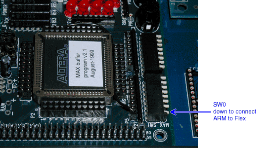
For more detail on the interface between the FLEX and the ARM, see memo 21.
The task for this week, and in fact for the whole project, is to interface the mouse to the ARM in such a way that pressing either mouse button causes the ARM to print the current "position" of the mouse in the debugger. The position must be an (X, Y) pair where X and Y are both signed 16 bit numbers. The lower 8 bits of the X value must also be written back from the ARM to the 7-segment LEDs of the FLEX when a mouse button is pressed. If both mouse buttons are pressed simultaneously then the program must terminate. Pressing button 1 of the Altera board must reset the mouse position to (0,0)—this will be useful for testing.
To do this you will need:
The program should only print the X and Y values when the buttons are first pressed, not while they are held down.
To allow the ARM to read data from the FLEX, you will need to do the following.
TRI tribuf0(my_data[0],enable_data_out,d[0]);
See Help | Primitives ... | TRI in MAX+Plus II for
a description of the TRI state module.
assign enable_data_out = !nOE && (your equations here);
Note that the ARM is configured to treat this bus as 8 bits wide so if you use ldr to load a 32 bit word the ARM will do four 8 bit reads on your behalf.
Hint: to multiplex a set of buses together you can use the ?: operator multiple times, e.g.:
    assign data_out = (select_bus == 2'd0) ? bus0 :
        (select_bus == 2'd1) ? bus1 :
        (select_bus == 2'd2) ? bus2 : bus3;
To avoid confusion and misunderstanding over the requirements, let me point out some obvious things to which you should nevertheless pay attention.
W4-Q1: the nWAIT line is being set to "z" in the supplied code, so basically we never drive it. Is there any difference between doing this and simply removing that line from both the Verilog and the .acf? Which is better? Explain your answer.
W4-Q2: this week we use the XCLK on pin 211 instead of the usual clock on pin 91. Why? Could we have used the old one instead? Why? Could we have used the XCLK in previous weeks? If no, why? If yes, why didn't we?
Submit your mini-report before the end of the last session of this week according to the usual rules (live demo, email submission, paper submission). Please don't leave this to the last moment: expect queues for the demonstrators' attention during the last hour, and remember that there are no more sessions after that, so no more chances to submit later.
Compose and submit your final report according to the rules on the main page. The very strict deadline for this is 17:00 on Friday 4 June 2004. The printed version goes to the Teaching Office, the electronic version to me by email.