Once the system has been placed and routed, the length and type of each conductor is known. These facts allow fairly accurate delay models of the conductors to be generated.
The accurate delay information is fed into the main simulator and the functionality of the chip or system is checked again. This is known as back annotation. It is possible that the new delays will prevent the system operating at the target clock frequency.
The marketing department have commonly pre-sold the product with an advertised clock frequency. Making the actual product work at this frequency is known as meeting timing closure.
The normal means to achieve timing closure is to migrate logic either side of an existing register or else to add a new register - but not all protocols are suitable for registering.
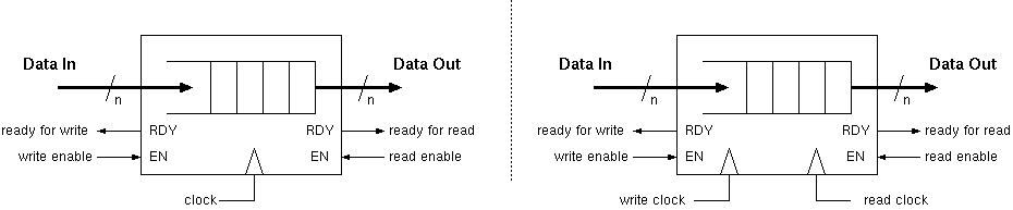
FIFOs are either synchronous or clock-domain crossing.
Synchronous FIFOs are either bubble-free (simultaneous read and write operations are always possible) or internally-pipelined (effect of a read or write is only visible at the opposite port a clock cycle later, also known as fully-registered). (Bluespec users' note: the default BSV FIFO is fully-registered and so introduces bubbles in both directions: it provides two variants with combinational paths which avoid bubbles in each direction respectively, called bypass and pipelined, but note that neither variant is fully-pipelined/fully-registered using the above definitions.)
A FIFO can help achieve timing closure, but again the protocol must be transactional and a bubble-free FIFO cannot always be used owing to its combinational path(s), hence latency is introduced.
| 48: (C) 2008-13, DJ Greaves, University of Cambridge, Computer Laboratory. | Flash Player Upgrade Needed |