Bump-in-Wire design for Microsoft Catapult Accelerator (2016).
Many hardware accelerator projects have ultimately been unsuccessful because: either
But by implementing accelerators on FPGA at a place where the data is moving already, these problems can be largely mitigated.
Also, until recently, FPGAs have not had hardened DRAM controllers and consequently been short of DRAM bandwidth.
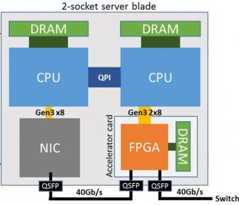
Microsoft have had several generations of blade design for their data centres. Recent ones have placed the FPGA in series with blade's network connection, thereby enabling copy-free pre- and post-processing of data. For instance, an index hash can be computed on database fields.
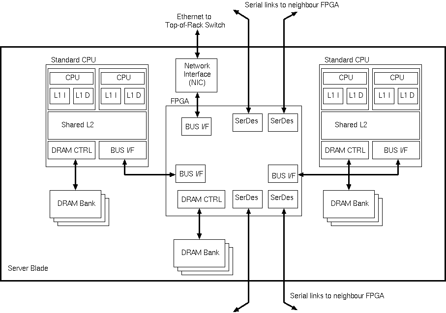
The FPGAs on neighbouring cards are also locally interconnected with a high-speed ring or mesh network, enabling them to be pooled and managed independently of the blade's CPUs. This enables systolic sorting networks and the like to be formed; e.g. for keeping the k-best Bing search results.
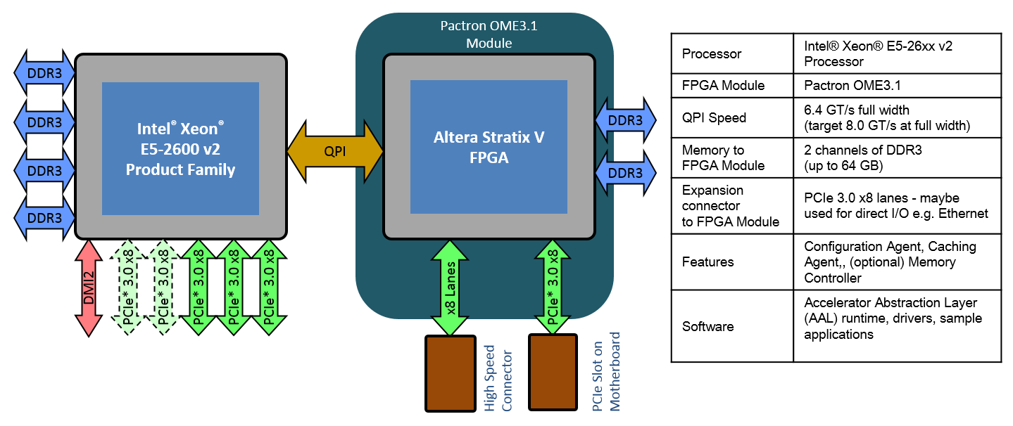
The QPI interconnection between CPUs is cache-consistent. Some FPGA-accelerated blade designs connect the FPGA to such a cache-consistent interconnect.
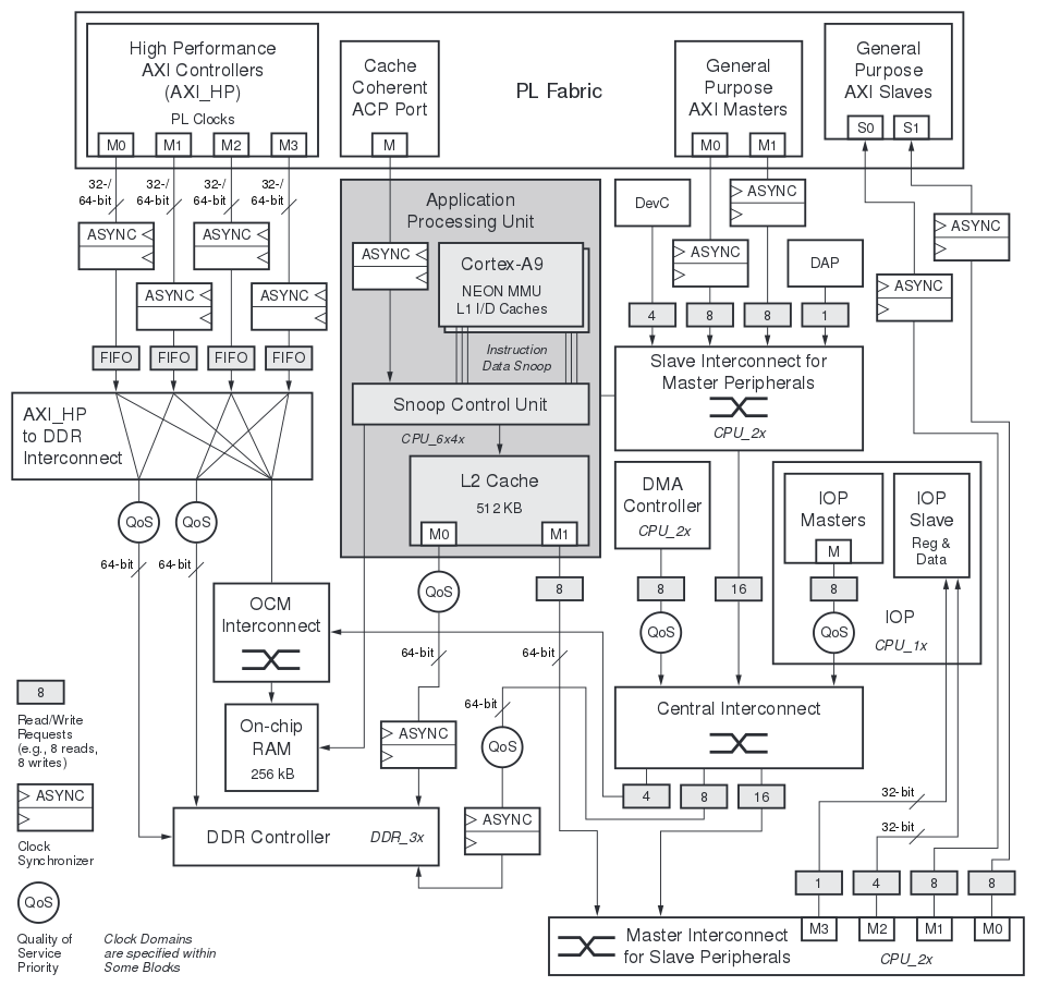
On the Zynq platform a number of methods for connecting to the reconfigurable logic are available - they are mostly via AXI ports. They vary in cache-consistency and bandwidth and initiator/target polarity.
| 4: (C) 2012-18, DJ Greaves, University of Cambridge, Computer Laboratory. |