The main datapaths within the ATM Camera V2 are shown in Figure 2.
Analogue video from the connectors on the front panel is digitised immediately, either as separate luminance and chrominance channels (for the SVHS case) or as a single PAL/NTSC composite signal. The digital sample stream is decoded by the Philips SAA7191 Digital Multistandard Decoder (Square Pixel) to produce a stream of 16-bit YUV pixels and all necessary horizontal and vertical sync signals. The decoder will automatically recognize PAL, NTSC or SECAM signals and adjust accordingly.
The output of the decoder passes into the SAA7186 Digital Video Scaler
chip which can take a specified rectangle of the input picture and
scale it to any smaller size. In addition, it can perform a number of
colour-space conversion functions. Typically the output from the
scaler chip is in the RGB colour-space since this it what most
frame-buffers require. Both the Decoder and Scaler are controlled by
the Microcontroller via an  bus.
bus.
The pixels from the scaler pass through an 24-bit wide SRAM large enough to hold 8 scan-lines of pixels. They are written into the SRAM in scan-line format and read out as 8x8 pixel tiles. At this point the data is written into video FIFOs large enough to store an entire frame. This allows the capture of the pixel data to proceed completely decoupled from its transmission across the ATM network interface.
The data from the VFIFOs may be transmitted as one of a number of uncompressed pixel formats by simple multiplexing of the bits, or may be passed through a JPEG compression engine (C-Cube CL550) to produce a variable-bit-rate stream.
A HI-FI audio Codec provides audio samples at a number of rates, in selctable formats up to 48kHz stereo 16 bit samples. The codec has 3 inputs and an output currently used for monitoring the capture channels.
The Microcontroller can also contruct cells for transmission over the ATM interface using registers provided within this Xilinx. This allows the MPU to transmit synchronization streams etc.
The bytes which result from all of these operations are marshalled into AAL5 PDUs by a Xilinx 3190 FPGA. The cell assembly takes place in a dual-ported SRAM.
Another Xilinx on the other side of the DPSRAM manages the ATM interface and is responsible for setting up the length, CRC32 and the header flag fields of each cell transmitted. This Xilinx supports four independent transmission channels:
Of the four channels, the MPU has priority to avoid the situation where control information is unable to get through due to the high bandwidth requirement of the ATM video streams.
On the AVA200 variant this Xilinx controls the two TAXI chips responsible for the ATM transmission interface. On the DAN variant the Xilinx presents the cell data directly to the switch fabric via two latches.
ATM Rx is also supported by the transmission Xilinx which provides a method for the MPU to read the 9-bit wide Rx FIFO. The 9th bit is used to tag the start of each cell. The microcontroller is interrupted when this FIFO is non-empty.
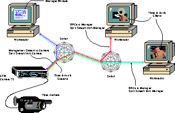
Figure 3: AVA200 Example System.