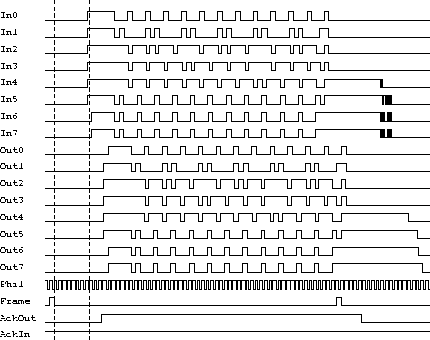
Figure 1 shows the timing diagram for a cell entering and leaving
a port controller (Phi1 is the clock). `Frame' pulses are generated as the
result of every  rising clock edge, and any device wishing to send
a cell into the fabric must generate the first byte of the cell (the routeing
byte) as a result of the eight rising clock edge after the one which created
the `frame' pulse, so that the fabric can latch that byte on the next rising
edge. i.e. it must be generated as result of the seventh rising clock edge
after the frame pulse is latched by the device. The dotted lines on figures
1 and 2 and the lines marked A and B on figure 3
show the rising clock edges which are used to latch the `frame' signal and
the first byte of the cell. They are 8 clock cycles appart.
rising clock edge, and any device wishing to send
a cell into the fabric must generate the first byte of the cell (the routeing
byte) as a result of the eight rising clock edge after the one which created
the `frame' pulse, so that the fabric can latch that byte on the next rising
edge. i.e. it must be generated as result of the seventh rising clock edge
after the frame pulse is latched by the device. The dotted lines on figures
1 and 2 and the lines marked A and B on figure 3
show the rising clock edges which are used to latch the `frame' signal and
the first byte of the cell. They are 8 clock cycles appart.
The ACK signal in this case is propagated from AckIn to AckOut as soon as the fabric decides that the cell has been routed successfully.
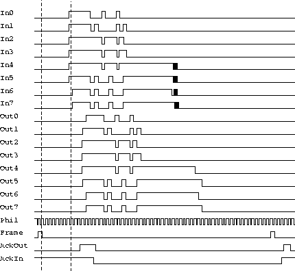
Figure 2: Timing Diagram (for a NACKed Cell)
Figure 2 shows the timing diagram for a cell, which has been NACKed,
entering and leaving a port controller. As before, the AckIn signal is
propagated through the fabric as it finishes the arbitration process. In this
case, however, the receiving circuit decides that it cannot accept the cell
(as a result of its FIFO being full) and therefore pulls AckIn low. This is
propagated to AckOut and the sending circuit aborts the cell after about 15
bytes.