The experiment was first performed on the lowliest of port controllers, `Sole', an ARM 3 powered device with an FCLK (CPU clock) speed of 25 MHz and MCLK (Memory system clock) of 8.33 MHz. The fabric back plane speed was 18 MHz. A range of burst sizes were tried yielding the following results:
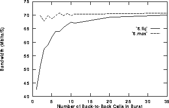
Figure 1:
Burst size versus Bandwidth for ARM 3 CPU, FCLK = 25 MHz, MCLK = 8.33 MHz, FABRIC = 18 MHz.
Note how as the burst size increases the CPU time is used more efficiently ie. the data rate required to cause it to stay in the FIQ is higher for larger burst sizes. Note how the `maximum sustainable throughput' figure is fairly constant over burst size. The larger bursts allow finer control over the data rate by the microsecond timer, and provide a more refined maximum figure.
Next, `Sole' was upgraded to use a 10 MHz MCLK. Since all FPC2s have 10 MHZ MEMCs (Memory Controllers), this could (and should) be done to all existing FPC2s. This represents the `standard' configuration for an FPC2, and is the most common amongst the ones we have.
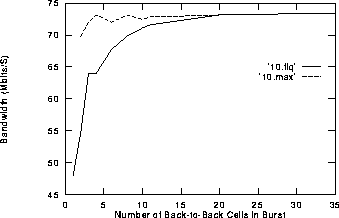
Figure 2:
Burst size versus Bandwidth for ARM 3 CPU, FCLK = 25 MHz, MCLK = 10.0 MHz, FABRIC = 18 MHz.
Increasing the MCLK speed by 20% resulted in a 4% improvement in maximum throughput. This was thought quite disappointing, given that it was thought that the CPU was bound by memory accesses. This was apparently the case for Xi2 bits, but Xi3 bits requires fewer memory cycles. Note however how faster memory accesses speed up the FIQ context switch time, resulting in a sharper FIQ curve.
There exists a ceramic version of the ARM 3 CPU that is rated at 30 MHz and was used in the next experiment. With a 10 MHz MCLK it was found to achieve a maximum sustainable throughput of 76.8 Mb/s. This is 5% better than the 25 MHz ARM 3 with the same 10 MHz MCLK. Again this was a little surprising as a more dramatic speed up was expected.
Future port controller such as FPC3 will use ARM 6xx CPUs. There exists a single ARM 600 FPC2 that was used for this experiment. The ARM 6 has basically the same processor core as the ARM 3, except for a 32 bit address space. Instruction execution times are the same, and they both implement the same write through cache. The advantage of the ARM 600 is that it has an eight entry write buffer, which allows the CPU to continue working at FCLK speeds while writes are pending rather than having to slow to MCLK speeds on every write.
Due to a beta silicon bug on our ARM 600, we were only able to run MCLK at 8.33 MHz. FCLK was set at the maximum 25 MHz, the same as for ARM 3s. As can be seen from the results, the write buffer really does make a difference. In fact, the ARM 600 is sufficiently fast such that the FIQ code is no longer the bottle neck. The failure of the FPC2 in cell forwarding above 82.5 Mb/s is in fact due to a hardware failure of the Xi3 bits when operating at 18 MHz. At this speed they are unable to read data from the transmission line FIFO fast enough to avoid it filling.
This problem could only be fixed by up-rating the fabric speed to  19.1
MHz, where the Xilinx would be able to drain the FIFO at the full 87.3
Mb/s transmission line rate. Faster Xilinx designs capable of 20 MHz
operation have been produced in the past, and probably could be again.
The reason for this not being done is that it was not holding anyone's
research up, and nothing was avaliable that could generate (or more to
the point, receive) at such high data rates.
19.1
MHz, where the Xilinx would be able to drain the FIFO at the full 87.3
Mb/s transmission line rate. Faster Xilinx designs capable of 20 MHz
operation have been produced in the past, and probably could be again.
The reason for this not being done is that it was not holding anyone's
research up, and nothing was avaliable that could generate (or more to
the point, receive) at such high data rates.
A summary of throughput results follows:
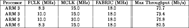
Table 1: Maximum Sustainable Throughput figures
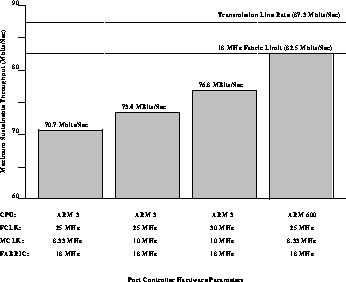
Figure 3:
Maximum Sustainable Throughput for Various Configurations.