Extracting a 3DES key from an IBM 4758Part 2: What is an FPGA ?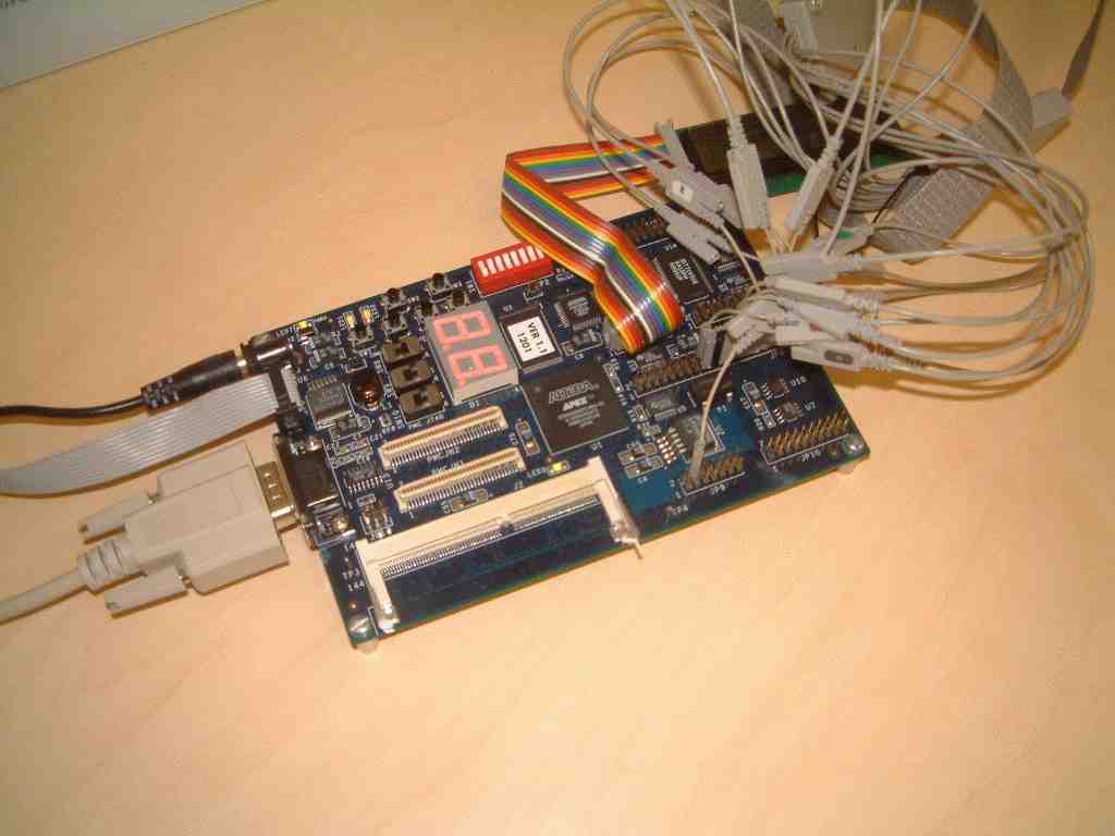
Photo of Altera's Excalibur development board A Field Programmable Gate Array (FPGA) is an integrated circuit whose functionality can be programmed in the field after manufacture. FPGA capacities have been growing year after year and modern devices can provide two million gate designs in a single chip. This is about the level of complexity of the first Intel Pentium microprocessors. When originally introduced FPGAs only had a handful of gates and designs were specified as logic equations connecting them up. Nowadays they are programmed in high level Hardware Description Languages (HDLs) such as Verilog1 , which superficially resembles high level programming languages such as C. For example, a linear feedback shift register might be expressed as:
   always @(posedge clk)
   begin
      count[73:0] <= count[74:1];
      count[74]   <= count[26] ^ count[23] ^ count[21] ^ count[19];
   end
The great advantage of an FPGA is the fast development time and very low cost of design cycles. Instead of spending thousands of dollars and waiting weeks for your design to come back from the fabrication plant you can program the FPGA, test it, and if you've made an error then within a few minutes you can fix the problem and reprogram the same device with a corrected design. Of course, an FPGA is only one part of a working system, which will need memory, connectors, a circuit board and a power supply. For the DES cracking project we avoided all the hard work of creating such a system by using an off-the-shelf development board, part of an 'Excalibur' kit2 from Altera3. Altera kindly provided ours for free (thanks!), but they'd be happy to sell you one for just $995. If you want to build your own circuit board then the chip will cost you from $178 upwards (one off) 4 though Altera suggest volume pricing will be about $5 5 [this sort of price differential for one off devices is typical for the industry]. The Excalibur system includes all the tools you need for programming the FPGA. You'll also need to provide your own PC to run the tools -- we used an 800MHz Windows 2000 system with 512MB of RAM. Speed is less important than RAM because otherwise the tools swap continuously and run very slowly indeed! The kit provides the design for a small microprocessor called a NIOS 6 (indeed the Excalibur board we used is intended for evaluation and development of NIOS based designs). The NIOS occupies about 20% of the FPGA leaving the rest for problem specific logic. This is a very powerful technique because it allows hardware to be used for the performance critical parts of a design and software running on the NIOS can be used to glue it together and communicate with the outside world.
Next part: What are DES and 3DES ?
Links1 Verilog 2001 http://www.verilog-2001.com/ 2 Excalibur Development Kit, Featuring NIOS http://www.altera.com/products/devices/excalibur/exc-kit.html 3 Altera Inc http://www.altera.com/ 4 Arrow Electronics Inc http://www.arrow.com/ 5 Altera Introduces The NiosTM Embedded Processor, Industry's First RISC-Based Embedded Processor Developed for SOPC Integration http://www.altera.com/corporate/press_box/releases/past/2000/pr_ex_nios.html 6 NIOS Embedded Processor http://www.altera.com/products/devices/excalibur/exc-nios_index.html |