⇡ Tutorial for the v0.4 lowRISC release
lowRISC Minion internals
This lowRISC release introduces Minion cores, allowing I/O tasks to be offloaded from the Rocket. This goal is important because it provides a flexible platform to allow new and unusual devices to be supported. From Chapter 3: extract from Pulpino databook
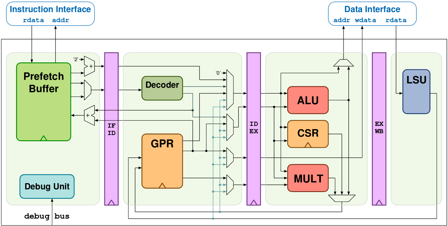
RISCV core overview from Pulpino databook
The Pulpino as delivered from ETH Zurich is a complete microcontroller, and as such is too large to support our FPGA platform. AXI-compatible busses and peripherals increase the size by 2-3 times. Consequently the decision was taken to only use the core of the previous system, now combined with some key new peripherals:
- Program RAM (64K, tightly coupled)
- Data RAM (64K, tightly coupled)
| Name | Address | Operation | Reset value | Description |
|---|---|---|---|---|
| Program RAM | 0x00000000 |
Read/Write | Boot program | The initial bootstrap program that can talk to the Rocket |
| Data RAM | 0x00100000 |
Read/Write | Bitstream | Any static data the bootstrap program might need |
| UART control | 0x00200000 |
Read/Write | zero | The UART can only be used if a separate POD interface is purchased |
| UART status | 0x00300000 |
Read/Write | zero | “ |
| SD RX FIFO | 0x00400000 |
Read/Write | zero | SD-card data will be received via this FIFO |
| SD TX FIFO/stat | 0x00500000 |
Read/Write | zero | SD-card data will be pre-loaded via this FIFO before a transaction |
| SD control/stat | 0x00600000 |
Read/Write | zero | The SD-card IO subsystem is controlled via these registers |
| LED ctrl/DIP sw | 0x00700000 |
Read/Write | zero | Write to LED and/or read from DIP switches |
| Shared memory | 0x00800000 |
Read/Write | zero | An 8K byte window that can be read/written by Minion and Rocket |
| Keyboard intf | 0x00900000 |
Read/Write | zero | The PS/2 keyboard may be polled or read at this address |
| VGA text buffer | 0x00A00000 |
Read/Write | zero | The least significant byte in each 32-bit word is usable |
| N/A | 0x00B00000 |
Read/Write | zero | |
| N/A | 0x00C00000 |
Read/Write | zero | |
| N/A | 0x00D00000 |
Read/Write | zero | |
| N/A | 0x00E00000 |
Read/Write | zero | |
| Reserved | 0x00F00000 |
Read/Write | zero |
To prevent problems with speculative pre-fetching, no auto incrementing on peripherals is supported. Therefore an I/O address must be written to before it will yield its first item of data. Although I/O addresses are described as R/W, to save unnecessary hardware, most will not read back what was written.
| Name | Address | Operation | Reset value | Description |
|---|---|---|---|---|
| UART transmit | 0x00200000 |
Write | zero | Add a byte to the UART transmit FIFO (2K entries) |
| UART baud rate | `0x00200004 | Write | 87 | The UART baud rate is dependent on the overall system clock (20MHz) |
| UART advance FIFO | 0x00300000 |
Write | zero | The UART receive FIFO advances when this register is written to |
| UART status | 0x00300000 |
Read/Write | zero | “ |
The built-in UART (only accessible via extra PMOD device), uses a simple protocol. Only the receive side is buffered in this version. Majority voting is implemented to reduce the impact of noise in the environment.
| Name | Address | Operation | Reset value | Description |
|---|---|---|---|---|
| Key FIFO status | 0x00900000 |
Read/Write | zero | The PS/2 keyboard may be polled or read at this address |
| Key FIFO output | 0x00900000 |
Read/Write | zero | The PS/2 keyboard may be polled or read at this address |
The keyboard FIFO has a 512 word buffer on input, and returns the scan code as its LSB, ASCII representation (British keyboards only), as MSB. The conversion to international alphabets may be done under Linux using its usual facilities. No provision to overwrite the code page is provided in this release, though it would be trivial to implement in hardware. The status output gives the number of keys pending and other FIFO information (see minion_soc.sv). Writing an arbitrary value to this address advances the FIFO to the next character.
| Name | Address | Operation | Reset value | Description |
|---|---|---|---|---|
| VGA text buffer | 0x00A00000 |
Read/Write | zero | The least significant byte in each 32-bit word is usable |
The VGA compatible text display is straightforward in operation. No facility for hardware scrolling is offered, the font is a fixed ASCII-font without non-Roman support. No support for overwriting the font is provided though again, it would be trivial in hardware. The output is a fixed 1024x768 at 75Hz. The buffer is a fixed 16K bytes with a 64K memory map, of which only the LSB is used.
| Name | Address | Operation | Reset value | Description |
|---|---|---|---|---|
| Shared memory | 0x00800000 |
Read/Write | zero | An 8K byte window that can be read/written by Minion and Rocket |
The shared memory is 8K bytes, operated as 32-bit quantities on both sides of the interface. No provision for collision detection or interrupts is included in this release. The shared memory appears as an extension to the block memory of the Rocket, consequently it starts at 0x40010000 with the standard Chisel memory map. No detection of the presence of the shared memory is made by the Boot ROM, consequently to detect the presence of the Minion
| Name | Address | Operation | Reset value | Description |
|---|---|---|---|---|
| SD rx current FIFO | 0x00400000 |
Read | zero | The SD receive FIFO returns its top item when this register is read |
| SD rx advance FIFO | 0x00400000 |
Write | zero | The SD receive FIFO advances when this register is written to |
| SD rx status | 0x00500000 |
Read | zero | The SD-card status is returned (legacy location) |
| SD tx load FIFO | 0x00500000 |
Write | zero | The SD transmit FIFO receives data when this register is written to |
| SD align reg | 0x00600000 |
Write | zero | Sector align register (not currently used) |
| SD clock din | 0x00600004 |
Write | zero | The data input pin for the SD-clk divider protocol |
| SD argument | 0x00600008 |
Write | zero | The SD-card command argument (such as sector offset for reads) |
| SD command | 0x0060000C |
Write | zero | The SD-card command number (such as reset/inquire/read/write) |
| SD setting | 0x00600010 |
Write | zero | The SD-card setting (short/long/with data/read/write) |
| SD start | 0x00600014 |
Write | zero | The SD-card command start register |
| SD reset | 0x00600018 |
Write | zero | The SD-card reset control (clock, data or command) |
| SD blkcnt | 0x0060001C |
Write | zero | The SD-card number of blocks (currently ignored) |
| SD blksize | 0x00600020 |
Write | zero | The SD-card block size (must be 512 except for inquiry commands) |
| SD timeout | 0x00600024 |
Write | zero | The SD-card timeout for command and data responses (in clocks) |
| SD clock crtl | 0x00600028 |
Write | zero | The SD-card clock divider control register (not supported in s/w) |
| SD resp[38:7] | 0x00600000 |
Read | zero | The SD-card response register |
| SD resp[70:39] | 0x00600004 |
Read | zero | The SD-card response register |
| SD resp[102:71] | 0x00600008 |
Read | zero | The SD-card response register |
| SD resp[133:103] | 0x0060000C |
Read | zero | The SD-card response register |
| SD cmd wait | 0x00600010 |
Read | zero | The SD-card actual waiting time for the last command |
| SD status | 0x00600014 |
Read | zero | The SD-card FIFO and state-machine status |
| SD packet[31:0] | 0x00600018 |
Read | zero | The SD-card last command packet sent (including CRC) |
| SD packet[47:32] | 0x0060001C |
Read | zero | The SD-card last command packet sent (including CRC) |
| SD data wait | 0x00600020 |
Read | zero | The SD-card actual waiting time for the last data transfer |
| SD transf cnt | 0x00600024 |
Read | zero | The SD-card number of 32-bit words transferred in a transaction |
| SD rx FIFO stat | 0x00600028 |
Read | zero | The SD-card receive FIFO status |
| SD tx FIFO stat | 0x0060002C |
Read | zero | The SD-card transmit FIFO status |
| SD card detect | 0x00600030 |
Read | zero | The SD-card present status |
| N/A | 0x00600034 |
Read | 0xDEADBEEF |
Unused |
| N/A | 0x00600038 |
Read | 0xDEADBEEF |
Unused |
| SD clock dout | 0x0060003C |
Read | zero | The SD-card clock divider response register (not supported in s/w) |
| SD align reg | 0x00600040 |
Read | zero | The SD-card delayed alignment register readback |
| SD clock din | 0x00600044 |
Read | zero | The SD-card delayed clock divider data input readback |
| SD argument | 0x00600048 |
Read | zero | The SD-card delayed argument readback |
| SD command | 0x0060004C |
Read | zero | The SD-card delayed command readback |
| SD setting | 0x00600050 |
Read | zero | The SD-card delayed setting readback |
| SD start | 0x00600054 |
Read | zero | The SD-card delayed start readback |
| SD reset | 0x00600058 |
Read | zero | The SD-card delayed reset readback |
| SD blkcnt | 0x0060005C |
Read | zero | The SD-card delayed block count readback |
| SD blksize | 0x00600060 |
Read | zero | The SD-card delayed block size readback |
| SD timeout | 0x00600064 |
Read | zero | The SD-card delayed timeout readback |
| SD clock ctrl | 0x00600068 |
Read | zero | The SD-card delayed clock control readback |
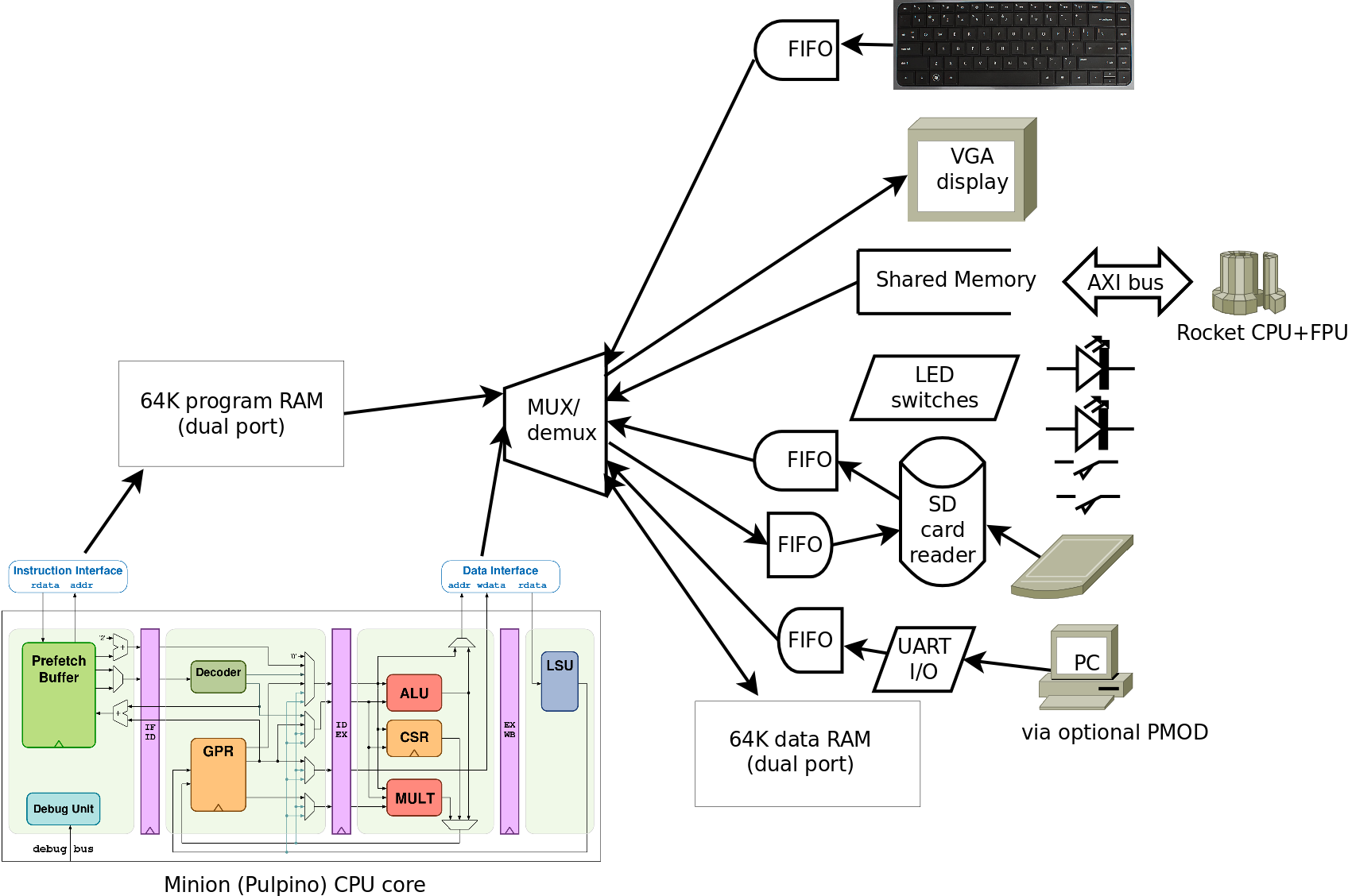
Minion core connectivity
For details of the SD-protocol, it may be helpful (caution: redacted information) to refer to the SD-association website.