HOME
UP
PREV
FURTHER NOTES
NEXT (Deep Submicron and Dark Silicon)
90 Nanometer Gate Length.
The mainstream VLSI technology in the period 2004-2008 was 90 nm. This had low leakage and very high wafer yields.
Now the industry is using 22 nanometer and smaller.
Parameters from a 90 nanometer standard cell library:
| Parameter | Value | Unit |
| Drawn Gate Length | 0.08 | µm |
| Metal Layers | 6 to 9 | layers |
| Max Gate Density | 400K | gates/mm² |
| Finest Track Width | 0.25 | µm |
| Finest Track Spacing | 0.25 | µm |
| Tracking Capacitance | 1 | fF/mm |
| Core Supply Voltage | 0.9 to 1.4 | V |
| FO4 Delay | 51 | ps |
| Leakage current | | nA/gate |
| 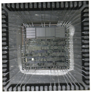 |
Typical processor core: 200k gates + 4 RAMs: one square millimeter.
Typical SoC chip area is 50-100 mm² → 20-40 million gates (semi-custom/standard cell).
Actual gate and transistor counts are higher owing to full-custom blocks (RAMs mainly).
- 2007: Dual-core Intel Itanium2: 1.6 billion transistors (90 nm).
- 2010: 8-core Intel Nehalem: 2.3 billion transistors (45 nm).
- 2010: Altera Stratix IV FPGA: 2.5 billion transistors (40 nm).
- 2015: Intel CPU: circa 10 billion transistors (19 nm).
- 2018:
»ITRS predicts 7 nm technology for this year (2018)!
» Moore's Law » Transistor Count »Dennard Scaling
»Dimension Increase in Metal-Oxide-Semiconductor Memories and Transistors
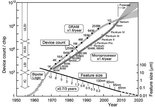
Technology Scaling Prediction.
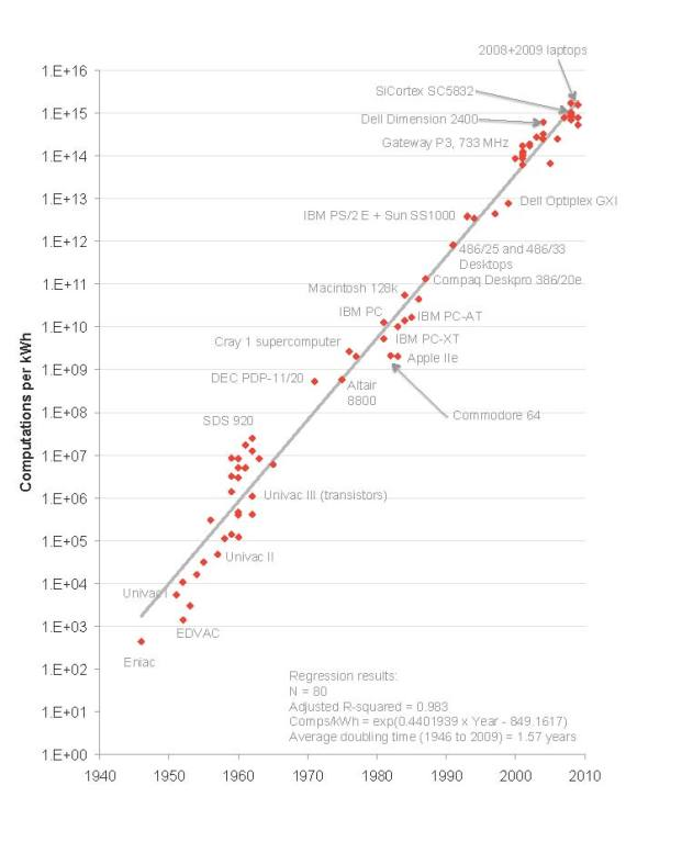
Computations per kWh. Divide by 3.6E6 for per Joule.
Dennard's Rule stated that as transistors get smaller, their power density stays constant, so that the power use stays in proportion with area: both voltage and current scale (downward) with length.
This meant that no new heat extraction technology was needed as VLSI capabilities improved.
But once a supply voltage of 1 volt was reached, silicon CMOS cannot be run at much lower voltages without leakage (static power) greatly increasing.
Typical modern datasheet rubric:
"The Xilinx Kintex UltraScaleTM FPGAs are available in -3, -2, -1, and -1L speed grades, with -3 having the
highest performance. The -1L devices can operate at either of two VCCINT voltages, 0.95V and 0.90V and
are screened for lower maximum static power. When operated at VCCINT = 0.95V, the speed specification
of a -1L device is the same as the -1 speed grade. When operated at VCCINT = 0.90V, the -1L performance
and static and dynamic power is reduced."