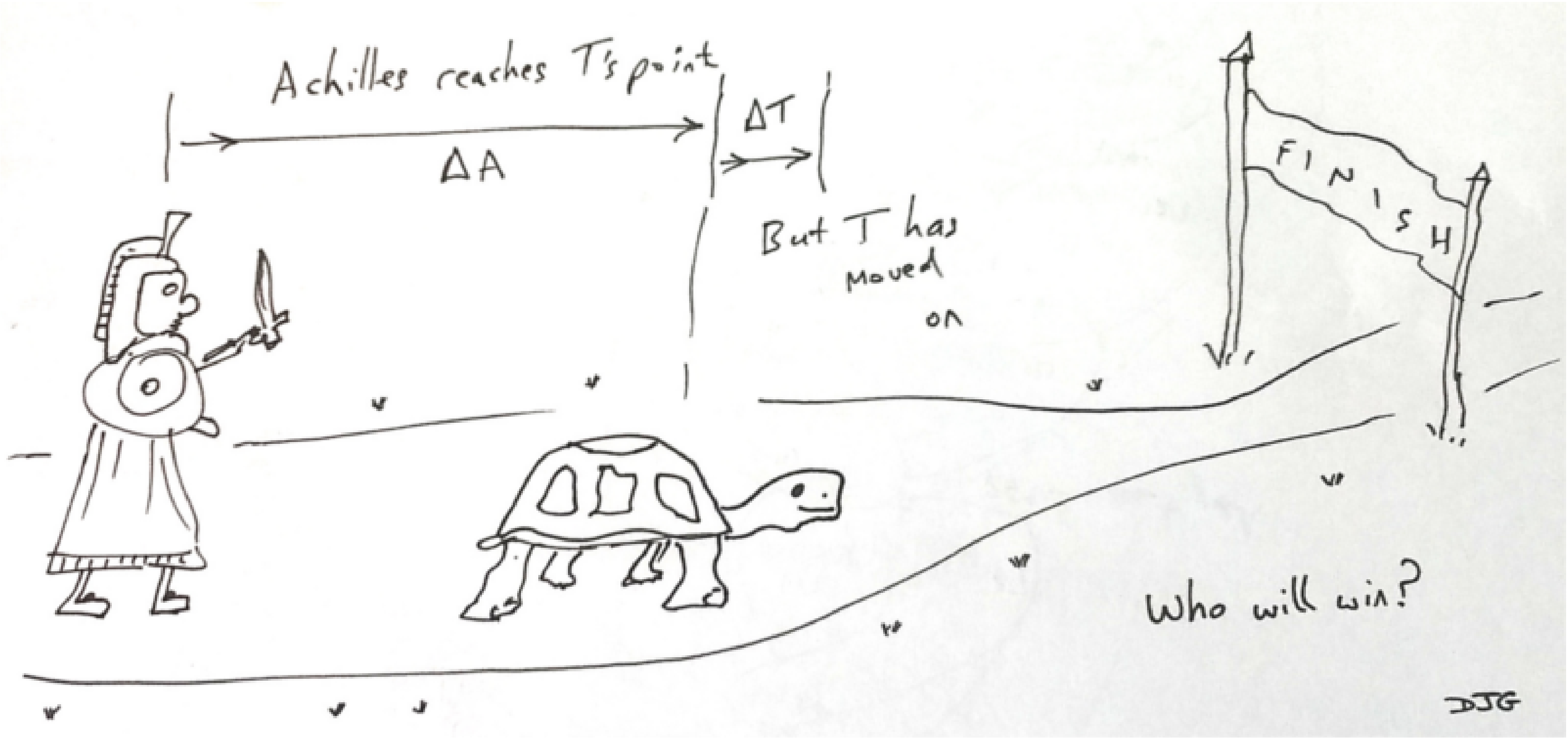
The book is externally available as an ePDF from the Arm web site for free or in hardcopy from Amazon etc..
Full text local access download (via Raven or equivalent): https://www.cl.cam.ac.uk/~djg11/pubs/modern-soc-design-djg/msd-private/DJG-Modern-SoC-Design-On-Arm-First-Edition.pdf PDF (607 pages).
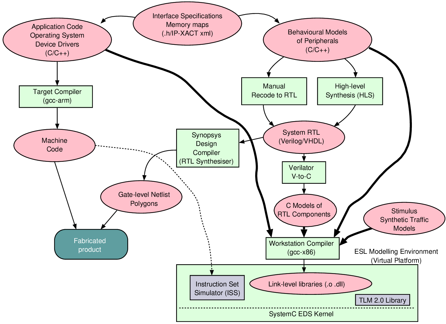
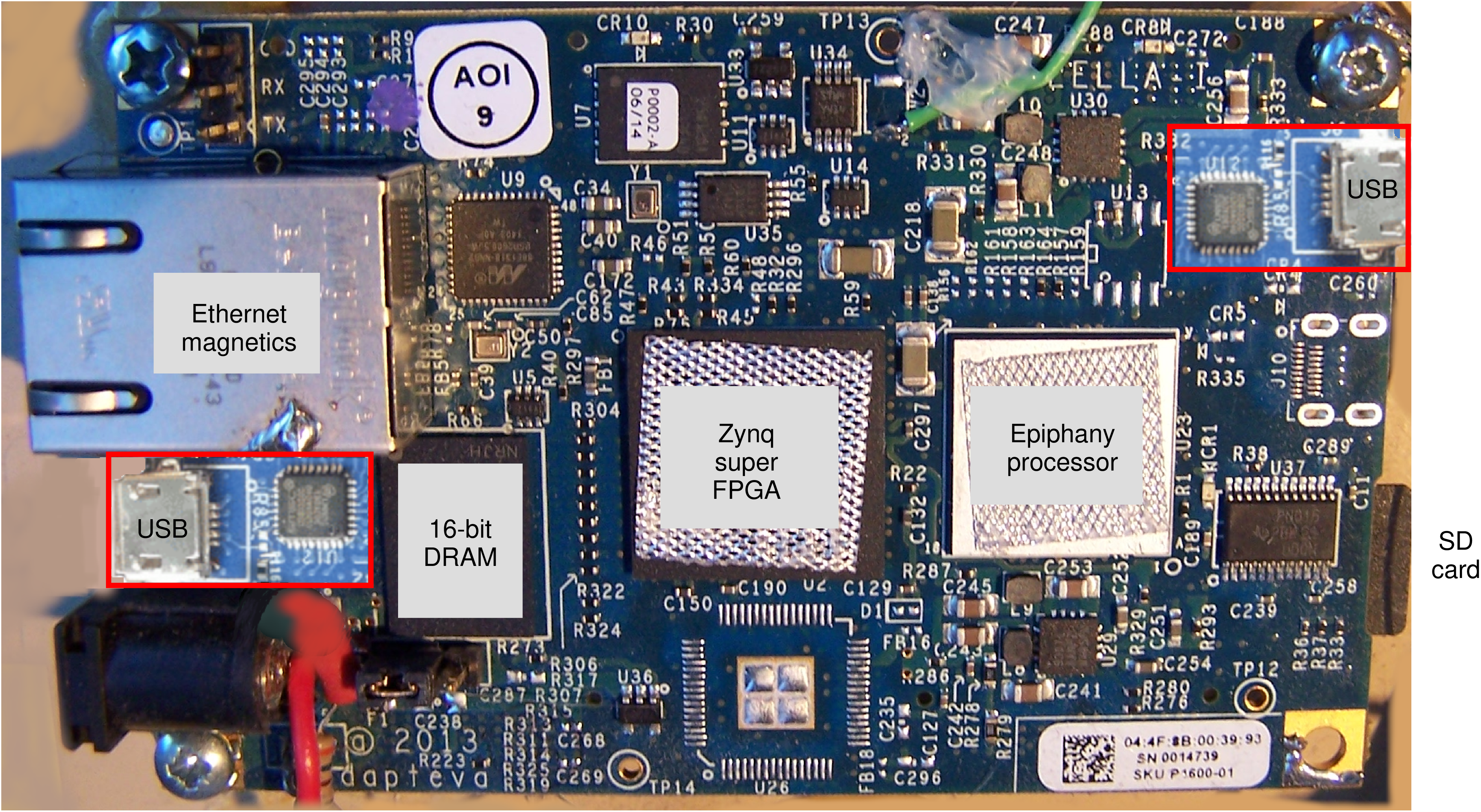
Many of the principles taught in this book are relevant for all forms of system architect, including those who are designing cloud-scale applications, custom accelerators or IoT devices in general, or those making FPGA designs. But the details of design verification in Chapter 8 are likely to be just of interest to those designing semi-custom silicon using standard cells. A git repository of online additional material is available at bitbucket.org/djg11/modern-soc-design-djg. This contains data used for generating tables and graphs in the book, as well as further source code, lab materials, examples and answers to selected exercises. The repo contains a SystemC model of the Zynq super FPGA device family, coded in blocking TLM style. It is sufficient to run an Arm A9 Linux kernel using an identical boot image as the real silicon. Published by Arm Education Media, 605 pages in softback and ePDF. ISBN 978-1-911531-36-4
https://www.cl.cam.ac.uk/ djg11/pubs/modern-soc-design-djg/
temp   := 200                 // Set initial temperature to a high value
ans    := first_guess         // This is the design vector (or tree)
metric := metric_metric ans   // We seek the highest-metric answer

while (temp > 1)
{
   // Create new design point, offsetting with delta proportional to temperature
   ans’ := perturb_ans temp ans

   // Evaluate (scalar) objective function (figure of merit) for new design point
   metric’ := metric_metric ans’

   // Accept if better probabilistically
   accept := (metric’ > metric) || rand(100..200) < temp;
   if (accept) (ans, metric, temp) := (ans’, metric’, temp * 0.99)
}
return ans;
| Label | Start address (hex) |
| g_drmp3_pow43-0x120 | 0x0000 |
| g_drmp3_pow43> | 0x120 |
| g_scf_partitions.6678> | 0x0c40 |
| … | |
| _end_of_static | 0x2350 |
| Event type | Number of operations |
| Input bytes | 16 392 |
| Output frames | 44 352 |
| DCT operations | 154 |
| Floating-point adds and subtracts | 874 965 |
| Floating-point multiplies | 401 255 |
| Integer adds and subtracts | 162 107 |
| Integer multiplies | 88 704 |
| Type | Data latency | Ready latency | Combinational paths |
| Fully registered | 1 | 1 | None |
| Bypass | 0 | 1 | WR_EN |
| Pipelined | 1 | 0 | RD_EN |
| Bubble-free | 0 | 0 | Both directions |
| Asynchronous | Several | Several | None |
| Credit-controlled | 1 | n/a | None |


| Device name | VU31P | VU33P | VU35P | VU37P | VU11P | VU13P |
| System logic cells (k) | 962 | 962 | 1907 | 2852 | 2835 | 3780 |
| CLB flip-flops (k) | 879 | 879 | 1743 | 2607 | 2592 | 3456 |
| CLB LUTs (k) | 440 | 440 | 872 | 1304 | 1296 | 1728 |
| Maximum distributed RAM (Mb) | 12.5 | 12.5 | 24.6 | 36.7 | 36.2 | 48.3 |
| Total block RAM (Mb) | 23.6 | 23.6 | 47.3 | 70.9 | 70.9 | 94.5 |
| Ultra RAM (Mb) | 90.0 | 90.0 | 180.0 | 270.0 | 270.0 | 360.0 |
| HBM DRAM (GB) | 4 | 8 | 8 | 8 | – | – |
| Clock management tiles | 4 | 4 | 5 | 3 | 6 | 4 |
| DSP slices | 2880 | 2880 | 5952 | 9024 | 9216 | 12 288 |
| PCIe ports | 4 | 4 | 5 | 6 | 3 | 4 |
| CCIX ports | 4 | 4 | 4 | 4 | – | – |
| 150G Interlaken | 0 | 0 | 2 | 4 | 6 | 8 |
| 100G Ethernet with RS-FEC | 2 | 2 | 5 | 8 | 9 | 12 |
| Maximum single-ended I/O | 208 | 208 | 416 | 624 | 624 | 832 |
| Multi-standard Gbps SERDES | 32 | 32 | 64 | 96 | 96 | 128 |
| L1 | L2
| |||||||||
| Cache | ||||||||||
| Size | Energy | Area | Hit rate | Access time | Mean time | Energy | Area | Hit rate | Access time | Mean time |
| 1 | 0.01 | 0.001 | 0.002 | 0.0 | 200 | 0.001 | 0.001 | 0.002 | 0.1 | 200 |
| 2 | 0.02 | 0.002 | 0.004 | 0.0 | 199 | 0.002 | 0.002 | 0.004 | 0.1 | 199 |
| 4 | 0.04 | 0.004 | 0.008 | 0.0 | 198 | 0.004 | 0.004 | 0.008 | 0.2 | 198 |
| 8 | 0.08 | 0.008 | 0.015 | 0.0 | 197 | 0.008 | 0.008 | 0.015 | 0.3 | 197 |
| 16 | 0.16 | 0.016 | 0.030 | 0.0 | 194 | 0.016 | 0.016 | 0.030 | 0.4 | 194 |
| 32 | 0.32 | 0.032 | 0.059 | 0.1 | 188 | 0.032 | 0.032 | 0.059 | 0.6 | 188 |
| 64 | 0.64 | 0.064 | 0.111 | 0.1 | 178 | 0.064 | 0.064 | 0.111 | 0.8 | 178 |
| 128 | 1.28 | 0.128 | 0.200 | 0.1 | 160 | 0.128 | 0.128 | 0.200 | 1.1 | 160 |
| 256 | 2.56 | 0.256 | 0.333 | 0.2 | 133 | 0.256 | 0.256 | 0.333 | 1.6 | 134 |
| 512 | 5.12 | 0.512 | 0.500 | 0.2 | 100 | 0.512 | 0.512 | 0.500 | 2.3 | 101 |
| 1024 | 10.24 | 1.024 | 0.667 | 0.3 | 67 | 1.024 | 1.024 | 0.667 | 3.2 | 69 |
| 2048 | 20.48 | 2.048 | 0.800 | 0.5 | 40 | 2.048 | 2.048 | 0.800 | 4.5 | 44 |
| 4096 | 40.96 | 4.096 | 0.889 | 0.6 | 23 | 4.096 | 4.096 | 0.889 | 6.4 | 28 |
| 8192 | 81.92 | 8.192 | 0.941 | 0.9 | 13 | 8.192 | 8.192 | 0.941 | 9.1 | 20 |
| 16 384 | 163.84 | 16.384 | 0.970 | 1.3 | 7 | 16.384 | 16.384 | 0.970 | 12.8 | 18 |
| 32 768 | 327.68 | 32.768 | 0.985 | 1.8 | 5 | 32.768 | 32.768 | 0.985 | 18.1 | 21 |
| 65 536 | 655.36 | 65.536 | 0.992 | 2.6 | 4 | 65.536 | 65.536 | 0.992 | 25.6 | 27 |
| 131 072 | 1310.72 | 131.072 | 0.996 | 3.6 | 4 | 131.072 | 131.072 | 0.996 | 36.2 | 37 |
| 262 144 | 2621.44 | 262.144 | 0.998 | 5.1 | 5 | 262.144 | 262.144 | 0.998 | 51.2 | 51 |
| L1 | L2 | L2 | Composite | Composite | Composite |
| size | size | energy | energy | area | mean time |
| 64 | 262 144 | 233.0 | 233.6 | 262.2 | 45.8 |
| 128 | 262 144 | 209.7 | 211.0 | 262.3 | 41.2 |
| 1024 | 262 144 | 87.4 | 97.6 | 263.2 | 17.4 |
| 4096 | 262 144 | 29.1 | 70.1 | 266.2 | 6.3 |
| Metric | Core complexity ( | DVFS voltage ( | Number of cores ( |
| Performance delivered | | | |
| Power used | | | |
| Increase in power for double performance | 4 | 8 | 2.16 |
# Unfold=1 is the baseline design. Unfold=3 uses three times more silicon.
static_dynamic_tradeoff <- function(clock_freq, leakage, unfold, xx)
{
  op_count <- 2e7;

  # Model: Pollack-like unfold benefit
  execution_time <- op_count / clock_freq / (unfold ^ 0.75);

  # Model: Higher supply needed for higher clock and leakage resistance slightly increasing with Vdd
  vdd <- 1 + 0.5 * (clock_freq/100e6);
  static_power <- leakage * vdd ^ 0.9 * unfold;

  # Integrate static power and energy
  static_energy <- static_power * execution_time;

  # Use CV^2 for dynamic energy
  dynamic_energy <- op_count * vdd ^ 2.0 * 5e-10;
}

//Output bit-to-byte buffer
void putbits(uint val, uint no_of_bits)
{
  buffer |= val << (int)no_of_bits;
  buffer_bits += no_of_bits;
  while (buffer_bits >= 8)
  { yield_byte((byte)(buffer & 0xFF));
    buffer_bits -= 8;
    buffer_bits >>= 8;
  }
}

// Send a DC component
void putDC(sVLCtable [] tab, int val)
{
  uint absval, size;
  absval = (uint) Math.Abs(val);
  /* Compute dct_dc_size */
  size = 0;
  while (absval!=0)
  { absval >>= 1;
    size ++;
  }
  // Generate VLC for dct_dc_size (B-12 or B-13)
  putbits(tab[size].code, tab[size].len);
  // Append fixed-length code (dc_dct_differential)
  if (size!=0) // Send val + (2 ^ size) - 1
  { if (val>=0) absval = (uint)val;
    else absval = (uint)(val + (1 << (int)size) - 1);
    putbits(absval, size);
  }
}

void putDClum(int val)
{
  putDC(DClumtab, val);
}

void putDCchrom(int val)
{
  putDC(DCchromtab, val);
}

void putAC(int run, int signed_level, int vlcformat)
{
    // ...
}
/* Generate variable-length codes for an intra-coded
   block (6.2.6, 6.3.17) */
void putintrablk(Picture picture, short [] blk, int cc)
{
  /* DC Difference from previous block (7.2.1) */
  int dct_diff = blk[0] - picture.dc_dct_pred[cc];
  picture.dc_dct_pred[cc] = blk[0];

  if (cc==0) putDClum(dct_diff);
  else putDCchrom(dct_diff);

  /* AC coefficients (7.2.2) */
  int run = 0;
  byte [] scan_tbl = (picture.altscan ? alternate_scan:
                      zig_zag_scan);
  for (int n=1; n<64; n++)
  { // Use appropriate entropy scanning pattern
    int signed_level = blk[scan_tbl[n]];
    if (signed_level!=0)
    {
      putAC(run, signed_level, picture.intravlc);
      run = 0;
    }
    else run++; /* count zero coefficients */
  }

  /* End of Block -- normative block punctuation */
  if (picture.intravlc!=0) putbits(6,4); // 0110 (B-15)
    else putbits(2,2); // 10 (B-14)
}

// Return difference between two (8*h) sub-sampled blocks
// blk1, blk2: addresses of top left pels of both blocks
// rowstride:  distance (in bytes) of vertically adjacent pels
// h:          height of block (usually 8 or 16)
int sumsq_sub22(byte [] blk1, byte [] blk2, int rowstride, int h)
{
  int ss = 0, p1 = 0, p2 = 0;
  for (int j=0; j<h; j++)
  {
    for (int i=0; i<8; i++)
    { int v = blk1[p1+i] - blk2[p2+i];
      ss += v*v;
    }
    p1+= rowstride; p2+= rowstride;
  }
  return ss;
}


   // Generator (src)
   while(1)
   {
     ch1 ! (x);
     x += 3;
   }
|
   // Processor
   while(1)
   {
     ch2 ! (ch1? + 2)
   }
|
// Consumer (sink) while(1) { $display(ch2?); } |
module mkTb1 (Empty);             // This module has no externally callable methods

   Reg#(int) rx <- mkReg (23);    // Create an instance of a 23-bit register called rx

   rule countone (rx < 30);       // A rule named ’countup’ with an explicit guard
      int y = rx + 1;             // This is short for int y = rx.read() + 1;
      rx <= rx + 1;               // This is short for rx.write(rx.read() + 1);
      $display ("countone: rx = %0d, y = %0d", rx, y);
   endrule

   rule counttwo (rx > 20);       // A competing rule, also guarded
      rx <= rx + 2;               // This increments twice each cycle
      $display ("counttwo: rx = %0d", rx);
   endrule

   rule done (rx >= 40);          // A third rule
      $finish (0);
   endrule

endmodule: mkTb1
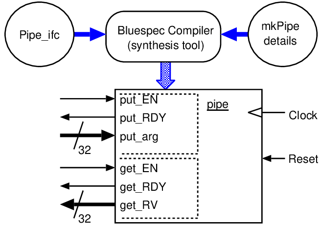
interface Pipe_ifc;
  method Action put(int arg);
  method int get();
endinterface
_________________________________________ module mkTb2 (Empty); // Testbench
Reg#(int) x <- mkReg (’h10);
Pipe_ifc thepipe <- mkPipe;
rule fill; // explicit guard of (true) is implied
thepipe.put(x);
// This is short for x.write(x.read() + ’h10);
x <= x + ’h10;
endrule
rule drain;
let y = thepipe.get();
$display (" y = %0h", y);
endrule
endmodule
|  |

// A simple long multiplier with
// variable latency
int multiply(int A, int B)
{
  int RA=A;
  int RB=B;
  int RC=0;
  while(RA>0)
  {
    if odd(RA) RC = RC + RB;
    RA = RA >> 1;
    RB = RB << 1;
  }
  return RC;
}
module LONGMULT8b8(clk, reset, C, Ready, A, B, Start);
   input clk, reset, Start;
   output Ready;
   input [7:0] A, B;
   output [15:0] C;
   reg [15:0] RC, RB, RA;
   reg        Ready;

   reg xx, yy, qq, pp; // Control and predicate nets
   reg [1:0] fc;
   reg [3:0] state;
   always @(posedge clk) begin
      xx = 0; // default settings.
      yy = 0;
      fc = 0;

      // Predicates
      pp = (RA!=16’h0);   // Work while pp holds
      qq = RA[0];         // Odd if qq holds

      if (reset) begin    // Sequencer
         state <= 0;
         Ready <= 0;
         end
      else case (state)
             0: if (Start) begin
                xx = 1;
                yy = 1;
                fc = 2;
                state <= 1;
             end

             1: begin
                fc = qq;
                if (!pp) state <= 2;
             end
             2: begin
                Ready <= 1;
                if (!Start) state <= 3;
             end

             3: begin
                Ready <= 0;
                state <= 0;
             end

           endcase // case (state)
      RB <= (yy) ? B: RB<<1;   // Data path
      RA <= (xx) ? A: RA>>1;
      RC <= (fc==2) ? 0: (fc==1) ? RC+RB: RC;
      end

   assign C = RC;
endmodule


  public static int associative_reduction_example(int starting)
  {
    int vr = 0;
    for (int i=0;i<15;i++) // or also i+=4
      {
      int vx = (i+starting)*(i+3)*(i+5); // Mapped computation
      vr ^= ((vx&128)>0 ? 1:0);          // Associative reduction
      }
    return vr;
  }
  double loop_carried_example(double seed, double arg0)
  {
    double vr = 0.0, vd = seed;
    for (int i=0;i<15;i++)
    {
        double vd = xf1(i*arg0);     // Parallelisable
        vd = xf2(vd + vd) * 3.14;    // Non-parallelisable
        vr += vd;
    }
    return vr;
  }
  static int [] foos = new int [10];
  static int ipos = 0;
  public static int loop_forwarding_example(int newdata)
  {
    foos[ipos ++] = newdata;
    ipos %= foos.Length;
    int sum = 0;
    for (int i=0;i<foos.Length-1;i++)
      {
      int dv = foos[i]^foos[i+1];  // Two adjacent locations are read
        sum += dv;                   // Associative scalar reduction in sum
      }
    return sum;
  }
  public static int data_dependent_controlflow_example(int seed)
  {
    int vr = 0;
    int i;
    for (i=0;i<20;i++)
      {
      vr += i*i*seed;
      if (vr > 1111) break; // Early loop exit
      }
    return i;
  }


SC_MODULE(mycounter) // An example of a leaf module (no subcomponents)
{
   sc_in  < bool       > clk, reset;
   sc_out < sc_int<10> > myout;

   void mybev()  // Internal behaviour, invoked as an SC_METHOD
   {
      myout =  (reset) ? 0: (myout.read()+1); // Use .read() since sc_out makes a signal
   }

   SC_CTOR(mycounter)        // Constructor
     { SC_METHOD(mybev);     // Require that mybev is called on each positive edge of clk
       sensitive << clk.pos();
     }
}
  int nv;                       // nv is a simple C variable (POD, plain old data)
  sc_out    < int > data;       // data and mysig are sc_signals (non-POD)
  sc_signal < int > mysig;      //
  ...
        nv += 1;
        data = nv;
        mysig = nv;
        printf("Before nv=%i, %i %i\n’’, nv, data.read(), mysig.read());
        wait(10, SC_NS);
        printf("After  nv=%i, %i %i\n’’, nv, data.read(), mysig.read());
  ...
Before nv=96, 95 95
After  nv=96, 96 96
SC_MODULE(mydata_generator)
{ sc_out < int  > data;
  sc_out < bool > req;
  sc_in  < bool > ack;

  void myloop()
  { while(1)
    { data = data.read() + 1;
      wait(10, SC_NS);
      req = 1;
      do { wait(10, SC_NS); } while(!ack.read());
      req = 0;
      do { wait(10, SC_NS); } while(ack.read());
    }
  }

  SC_CTOR(mydata_generator)
  {
    SC_THREAD(myloop);
  }
}
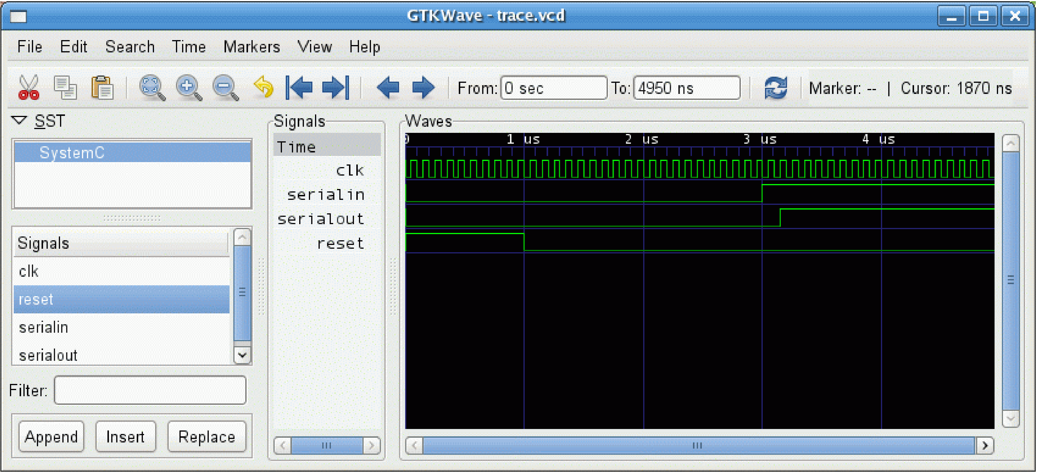
      sc_trace_file *tf = sc_create_vcd_trace_file("tracefilename");

      // Now call:
      // sc_trace(tf, <traced variable>, <string>);

      sc_signal < bool  > serialin("serialin"); // A named signal
      sc_signal < bool  > serialout;            // An unnamed signal
      float fbar;
      sc_trace(tf, clk);
      sc_trace(tf, serialin);
      sc_trace(tf, serialout, "serialout");     // Give name since not named above
      sc_trace(tf, fbar, "fbar");               // Give name since POD form

      sc_start(1000, SC_NS);                    // Simulate for 1 microsecond (old API)
      sc_close_vcd_trace_file(tr);
      return 0;
  sc_signal < bool > mywire; // Rather than a channel conveying just one bit

  struct capsule
  { int ts_int1, ts_int2;
    bool operator== (struct ts other)
    { return (ts_int1 == other.ts_int1) && (ts_int2 == other.ts_int2); }

    int next_ts_int1, next_ts_int2; // Pending updates
    void update()
    { ts_int1 = next_ts_int1; ts_int2 = next_ts_int2;
    }
    ...
    ... // Also must define read(), write() and value_changed()
  };

  sc_signal < struct capsule > myast; // We can send two integers at once
  void mymethod()  { .... }
  SC_METHOD(mymethod)
  sensitive << myast.pos(); // User must define concept of posedge for their own abstract type

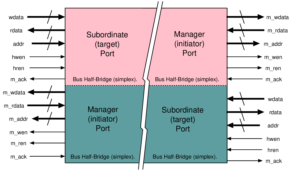
// Filling in the fields or a TLM2.0 generic payload:
  trans.set_command(tlm::TLM_WRITE_COMMAND);
  trans.set_address(addr);
  trans.set_data_ptr(reinterpret_cast<unsigned char*>(&data));
  trans.set_data_length(4);
  trans.set_streaming_width(4);
  trans.set_byte_enable_ptr(0);
  trans.set_response_status( tlm::TLM_INCOMPLETE_RESPONSE );

// Sending the payload through a TLM socket:
  socket->b_transport(trans, delay);
| simple_initiator_socket.h | A version of an initiator socket that has a default implementation of all interfaces. It allows the registration of an implementation for any of the interfaces to the socket, either unique interfaces or tagged interfaces (carrying an additional ID). |
| simple_target_socket.h | A basic target socket that has a default implementation of all interfaces. It also allows the registration of an implementation for any of the interfaces to the socket, either unique interfaces or tagged interfaces (carrying an additional ID). This socket allows only one of the transport interfaces (blocking or non-blocking) to be registered and implements a conversion if the socket is used on the other interface. |
| passthrough_target_socket.h | A target socket that has a default implementation of all interfaces. It also allows the registration of an implementation for any of the interfaces to the socket. |
| multi_passthrough_initiator_socket.h | An implementation of a socket that allows multiple targets to be bound to the same initiator socket. It implements a mechanism that allows the index of the socket the call passed through in the backward path to be identified. |
| multi_passthrough_target_socket.h | An implementation of a socket that allows multiple initiators to bind to the same target socket. It implements a mechanism that allows the index of the socket the call passed through in the forward path to be identified. |
  vqueue::b_transact(pkt, sc_time &delay)
  {
     // Measure utilisation and predict queue delay based on last 32 transactions
     if (++opcount == 32)
     {  sc_time delta = sc_time_stamp()+delay-last_measure_time;
        local_processing_delay += (delay_formula(delta/32)-local_processing_delay)/16;
        logging.log(25, delta);                  // record utilisation
        last_measure_time = sc_time_stamp()+delay;
        opcount = 0;
     }

     // Add estimated (virtual) queuing penalty
     delay += local_processing_delay;

     // Do actual work
     output.b_transact(pky, delay);
  }

void mips64iss::step()
{
  u32_t ins = ins_fetch(pc);
  pc += 4;
  u8_t opcode = ins >> 26;    // Major opcode
  u8_t scode = ins&0x3F;      // Minor opcode
  u5_t rs = (ins >> 21)&31;   // Registers
  u5_t rd = (ins >> 11)&31;
  u5_t rt = (ins >> 16)&31;

  if (!opcode) switch (scode) // decode minor opcode
  {
    case 052: /* SLT - set on less than */
      regfile_up(rd, ((int64_t)regfile[rs]) < ((int64_t)regfile[rt]));
      break;

    case 053: /* SLTU - set on less than unsigned */
      regfile_up(rd, ((u64_t)regfile[rs]) < ((u64_t)regfile[rt]));
      break;
      ...
   ...

void mips64iss::regfile_up(u5_t d, u64_t w32)
{ if (d != 0) // Register zero stays at zero
    { TRC(trace("[ r%i := %llX ]", d, w32));
      regfile[d] = w32;
    }
}
| Index | Type of ISS | I-cache traffic | D-cache traffic | Relative |
| modelled | modelled | performance | ||
| (1) | Interpreted RTL | Y | Y | 0.000001 |
| (2) | Compiled RTL | Y | Y | 0.00001 |
| (3) | V-to-C C++ | Y | Y | 0.001 |
| (4) | Handcrafted cycle-accurate C++ | Y | Y | 0.1 |
| (5) | Handcrafted high-level C++ | Y | Y | 1.0 |
| (6) | Trace buffer/JIT C++ | N | Y | 20.0 |
| (7) | Native cross-compile | N | N | 50.0 |
|
| Without simulation | Using simulation |
| Without place and route | Fast design exploration | Can generate indicative activity ratios that can be used instead of a simulation in further runs |
|
|
||
| With place and route | Static timing analyser will give an accurate clock frequency | Gold standard: only bettered by measuring a real chip |
    module CTR16(
      input mainclk,
      input din, input cen,
      output o);

      reg [3:0] count, oldcount;          // D-types

      always @(posedge mainclk) begin
          if (cen) count <= count + 1;    // ALU
          if (din) oldcount <= count;     // Wiring
          end

     assign o = count[3] ^ count[1];      // Combinational

   endmodule
| Parameter | Value |
| Fabrication geometry | 22 nm |
| Organisation | 64Kx64 |
| Nominal VDD | 1.0 V |
| Number of banks | 1 |
| Read/write ports per bank | 1 |
| Read ports per bank | 0 |
| Write ports per bank | 0 |

void sram64_cbg::recompute_pvt_parameters() // Called in constructor and when Vcc is changed
{
  m_latency =  sc_time(0.21 + 3.8e-4 *sqrt(float(m_bits)), SC_NS);

  pw_power leakage = pw_power(82.0 * m_bits, PW_nW);
  set_static_power(leakage);

  set_fixed_area(pw_area(13359.0 + 4.93/8 * m_bits, PW_squm));

  m_read_energy_op = pw_energy(5.0 + 1.2e-4 / 8.0 *m_bits, pw_energy_unit::PW_pJ);
  m_write_energy_op = 2.0 * m_read_energy_op; // rule of thumb!

  // NB: Might want different energy when high-order address bits change

  pw_voltage vcc = get_vcc();
  m_latency = m_latency / vcc.to_volts();
  cout << name () << ":" << kind() << ": final latency = " << m_latency << "\n";
}
void sram64_cbg::b_access(PW_TLM_PAYTYPE &trans, sc_time &delay)
{
  tlm::tlm_command cmd = trans.get_command();

  // Log wiring power consumed by transaction arriving here.
  // Also set which nets modelled by the TLM will be active after this operation:
  // For a write none (except a response ack) and for read the payload data.
  trans.pw_log_hop(this,  (cmd==tlm::TLM_READ_COMMAND ? PW_TGP_DATA: PW_TGP_NOFIELDS) |
          PW_TGP_ACCT_CKP,  &read_bus_tracker);

  if (cmd == tlm::TLM_READ_COMMAND)
    {
      // Log internal transaction energy for read
      pw_module_base::record_energy_use(m_read_energy_op);
      ...
    }
  else if (cmd == tlm::TLM_WRITE_COMMAND)
    {
      // Log internal transaction energy for write
      pw_module_base::record_energy_use(m_write_energy_op);
      ...
    }
}
| Device type | | Clock | Access | Activate | Read | Write |
| (capacity, word | frequency | time | ||||
| size and speed) | (cycles) | (MHz) | (ns) | (pJ) | (pJ) | (pJ) |
| DDR4_4Gb_x4_1866 | 13 | 934.6 | 32.1 | 4006.1 | 5752.3 | 6985.0 |
| DDR4_4Gb_x4_2133 | 16 | 1063.8 | 33.8 | 3754.0 | 5775.4 | 7219.2 |
| DDR4_4Gb_x4_2400 | 17 | 1204.8 | 31.5 | 4063.7 | 5418.2 | 7330.6 |
| DDR4_4Gb_x4_2666 | 19 | 1333.3 | 31.5 | 4104.0 | 6048.0 | 7488.0 |
| DDR4_8Gb_x4_1866 | 13 | 934.6 | 32.1 | 5156.5 | 5341.4 | 4930.6 |
| DDR4_8Gb_x4_2133 | 16 | 1063.8 | 33.8 | 5270.0 | 4692.5 | 4331.5 |
| DDR4_8Gb_x4_2666 | 19 | 1333.3 | 31.5 | 6105.6 | 4608.0 | 4089.6 |
| DDR4_8Gb_x4_2933 | 21 | 1470.6 | 31.3 | 6632.4 | 4595.7 | 4021.2 |
| DDR4_8Gb_x4_3200 | 22 | 1587.3 | 30.2 | 7136.6 | 4644.9 | 4015.9 |
| Operating mode | Rail 1 | Rail 2 | Rail 3 | Total power | |||
| (volts) | (mA) | (volts) | (mA) | (volts) | (mA) | (mW) | |
| Standby | 3.3 | 0.018 | 1.8 | 0.0007 | 3.3 | 0.03 | 0.16 |
| L/S mode | 3.3 | 6.3 | 1.8 | 11 | 3.3 | 5 | 57 |
| H/S mode | 3.3 | 29 | 1.8 | 22 | 3.3 | 59 | 155 |


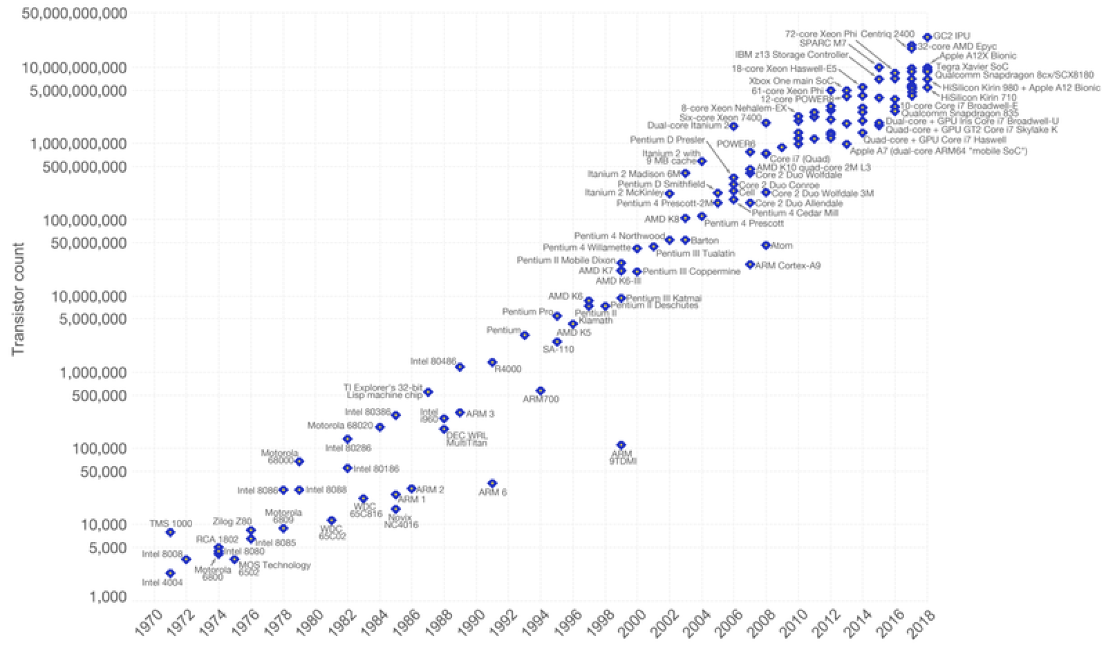
| Year introduced | Microprocessor | No of transistors | Geometry |
| 2007 | Dual-core Intel Itanium 2 | 1.6 billion | 90 nm |
| 2010 | 8-core Intel Nehalem | 2.3 billion | 45 nm |
| 2010 | Altera Stratix IV FPGA | 2.5 billion | 40 nm |
| 2015 | Intel CPU | circa 10 billion | 19 nm |
| 2020 | Nvidia’s GA100 Ampere | 54 billion | 7 nm |

| Year of production | 2015 | 2017 | 2019 | 2021 | 2024 | 2027 | 2030 |
| Logic device technology names | P70M56 | P48M36 | P42M24 | P32M20 | P24M12G1 | P24M12G2 | P24M12G3 |
| Logic industry node range label (nm) | 16/14 | 11/10 | 8/7 | 6/5 | 4/3 | 3/2.5 | 2/1.5 |
| Logic device structure | FinFET | FinFET | FinFET | FinFET | VGAA | VGAA | VGAA |
|
| FDSOI | FDSOI | LGAA | LGAA | M3D | M3D | M3D |
|
| VGAA | ||||||
|
| |||||||
| Device Electrical Specifications
| |||||||
| Power supply voltage, | 0.80 | 0.75 | 0.70 | 0.65 | 0.55 | 0.45 | 0.40 |
| Sub-threshold slope (mV/decade) | 75 | 70 | 68 | 65 | 40 | 25 | 25 |
| Inversion layer thickness (nm) | 1.10 | 1.00 | 0.90 | 0.85 | 0.80 | 0.80 | 0.80 |
| | 129 | 129 | 133 | 136 | 84 | 52 | 52 |
| | 351 | 336 | 333 | 326 | 201 | 125 | 125 |
| Effective mobility (cm | 200 | 150 | 120 | 100 | 100 | 100 | 100 |
| | 280 | 238 | 202 | 172 | 146 | 124 | 106 |
| Ballisticity: injection velocity (cm/s) | | | | | | | |
| | 0.115 | 0.127 | 0.136 | 0.128 | 0.141 | 0.155 | 0.170 |
| | 0.125 | 0.141 | 0.155 | 0.153 | 0.169 | 0.186 | 0.204 |
| | 2311 | 2541 | 2782 | 2917 | 3001 | 2670 | 2408 |
| | 1177 | 1287 | 1397 | 1476 | 1546 | 1456 | 1391 |
| | 1455 | 1567 | 1614 | 1603 | 2008 | 1933 | 1582 |
| | 596 | 637 | 637 | 629 | 890 | 956 | 821 |
| Cch, total (fF/µm | 31.38 | 34.52 | 38.35 | 40.61 | 43.14 | 43.14 | 43.14 |
| Cgate, total (fF/µm), HP logic | 1.81 | 1.49 | 1.29 | 0.97 | 1.04 | 1.04 | 1.04 |
| Cgate, total (fF/µm), LP Logic | 1.96 | 1.66 | 1.47 | 1.17 | 1.24 | 1.24 | 1.24 |
| CV/I (ps), FO3 load, HP logic | 3.69 | 2.61 | 1.94 | 1.29 | 1.11 | 0.96 | 0.89 |
| I/(CV) (1/ps), FO3 load, HP logic | 0.27 | 0.38 | 0.52 | 0.78 | 0.90 | 1.04 | 1.12 |
| Energy per switching (CV | 3.47 | 2.52 | 1.89 | 1.24 | 0.94 | 0.63 | 0.50 |


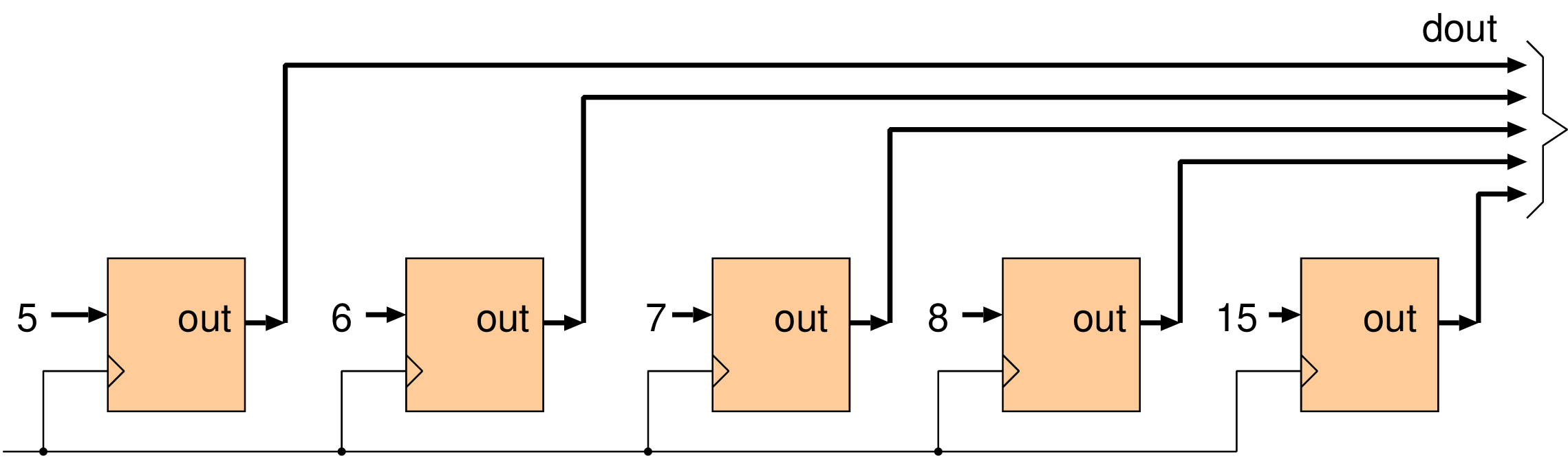
wire dout[39:0];
reg[3:0] values[0:4] = {5, 6, 7, 8, 15};

generate
  genvar i;
  for (i=0; i<5; i++)  begin
    MUT mut[i] (
    .out(dout[i*8+7:i*8]),
    .value_in(values[i]),
    .clk(clk),
    );
  end
endgenerate
|  |
module subcircuit(
  input clk,
  input rst,
  output q2);
   wire q1, q3, a;
   DFFR Ff_1(clk, rst, a, q1, qb1),
        Ff_2(clk, rst, q1, q2, qb2),
        Ff_3(clk, rst, q2, q3, qb3);
   NOR2 Nor2_1(a, q2, q3);
endmodule
|  |

 |  |
  reg [31:0] q, n;
  ...
  q = n / 10;
  return q;
|
reg [31:0] q, n; ... q = (n >> 1) + (n >> 2); q += (q >> 4); q += (q >> 8); q += (q >> 16); return q >> 3; |
| Parameter | Values |
| Process variation | 0.9 to 1.1 |
| Supply voltage range | 0.85 to 1.1 V |
| Temperature range | 0 to 70 |


      000 000 0 001 111 1
      123 456 7 890 123 4
    [ 00H 00H p H00 x00 p ]
    [ 01H 00H p H00 x00 p ]
    [ 10H 00H p H00 x00 p ]
    [ 11L 00H p H00 x00 p ]

module sewkit(  // TSMC 0.18u library
       intput clk,
       input n_reset);
    // verilint 630  on : Port connected to a NULL expression
    dfcfb1  DZBRB1_1(.CDN(n_reset), .CPN(clk), .D(1’b0), .Q(), .QN());
    dfcfb1  DZBRB1_2(.CDN(n_reset), .CPN(clk), .D(1’b0), .Q(), .QN());

    nd02d2  ND02D2_1 (.A1(1’b0), .A2(1’b0), .ZN() );
    nd02d2  ND02D2_2 (.A1(1’b0), .A2(1’b0), .ZN() );

    inv0d2  INV0D2_1(.I(1’b0), .ZN());
    inv0d2  INV0D2_2(.I(1’b0), .ZN() );
    inv0d2  INV0D4_1(.I(1’b0), .ZN() );
    inv0d2  INV0D4_2(.I(1’b0), .ZN() );

    buffd7  BUFFD1_1(.I(1’b0), .Z() );
    buffd7  BUFFD1_2(.I(1’b0), .Z() );

    mx02d2  MX02D1_1(.I0(1’b0), .I1(1’b0), .S(1’b0), .Z() );
    mx02d2  MX02D1_2(.I0(1’b0), .I1(1’b0), .S(1’b0), .Z() );

    nr02d2  NR02D2_1 (.A1(1’b0), .A2(1’b0), .ZN() );
    nr02d2  NR02D2_2 (.A1(1’b0), .A2(1’b0), .ZN() );

    aoi211d2 AOI311D1_1(.A(1’b0), .B(1’b0), .C1(1’b0), .C2(1’b0), .ZN() );
    aoi211d2 AOI311D1_2(.A(1’b0), .B(1’b0), .C1(1’b0), .C2(1’b0), .ZN() );
endmodule
| Type of expense | Item | Item cost | Total cost |
| NRE | 6 months: 10 software engineers | $100k pa | $500k |
| NRE | 6 months: 10 hardware engineers | $250k pa | $1250k |
| NRE | 4 months: 20 verification engineers | $200k pa | $1333k |
| NRE | 1 mask set (22 nm) | $1500k | $1500k |
| RE | Per device IP licence fees | ? | $?? |
| RE | 6-inch wafer | $5k | $5k |
| Total |
| $4583k + 5k |
|
| Area (mm | Number of wafer dies | Number of working dies | Cost per working die ($) |
| 2 | 9000 | 8910 | 0.56 |
| 3 | 6000 | 5910 | 0.85 |
| 4 | 4500 | 4411 | 1.13 |
| 6 | 3000 | 2911 | 1.72 |
| 9 | 2000 | 1912 | 2.62 |
| 13 | 1385 | 1297 | 3.85 |
| 19 | 947 | 861 | 5.81 |
| 28 | 643 | 559 | 8.95 |
| 42 | 429 | 347 | 14.40 |
| 63 | 286 | 208 | 24.00 |
| 94 | 191 | 120 | 41.83 |
| 141 | 128 | 63 | 79.41 |
| 211 | 85 | 30 | 168.78 |
| 316 | 57 | 12 | 427.85 |
| 474 | 38 | 4 | 1416.89 |
| String | Meaning |
| ss_0p9v_m40c | Slow P and N channel transistors at 0.9 V and |
| tt_1p0v_25c | Typical P and N channel transistors at 1.0 V and room temperature |
| ff_1p1v_125c | Fast P and N channel transistors at 1.1 V and 125°C |
| BEOL Corner | Meaning |
| C | Narrow wires with wide spacing for the smallest capacitance component |
| RC | Thick wires with less resistance to minimise the RC product and net delay |
| Typical | Wires and vias meet the target dimensions |
| RC | Thin wires with more resistance to maximise the RC product and net delay |
| C | Wide wires with narrow spacing for the largest capacitance component |
# ---- Create Clocks ----
create_clock -add -period $clock_period -name VCLK

foreach clock_name $clock_list {
  create_clock -add -period $clock_period [get_ports $clock_name] -name $clock_name
  set_clock_latency $clock_latency [get_clocks $clock_name]
}

set_clock_uncertainty [expr $setup_margin + $clock_jitter] -setup [all_clocks]
set_clock_uncertainty [expr $hold_margin]                  -hold  [all_clocks]

set_driving_cell -lib_cell $clock_driving_cell \
                 -input_transition_rise $max_clock_transition \
                 -input_transition_fall $max_clock_transition \
                 [get_ports $clock_list]

# ---- I/O timing constraints ----
set_input_delay $max_input_constraint -max -clock VCLK \
             [remove_from_collection [all_inputs] $clock_list]
set_input_delay $min_input_constraint -min -clock VCLK \
             [remove_from_collection [all_inputs] $clock_list]

set_output_delay $max_output_constraint -max -clock VCLK [all_outputs]
set_output_delay $min_output_constraint -min -clock VCLK [all_outputs]

# ---- Path groups ----
group_path -name reg2reg -from [all_registers] -to [all_registers]

# ---- Timing exceptions ----
set_multicycle_path 2 -setup -end -from [get_ports DFT*]
set_multicycle_path 1 -hold  -end -from [get_ports DFT*]
%
% # ---- Scan mode ----
%\end{verbatim}}
   assert(x<4);
   x := x + 1000;
   assert(x<1004);

| Syntax | Fundamental | Description |
| {A;B} | Core | Semicolon denotes sequence concatenation |
| {A[*]} | Core | A postfix asterisk denotes arbitrary repetition |
| {A | Core | Vertical bar (stile) denotes alternation |
| {A[+]} | Derived | One or more occurrences of A |
| {A[*n]} | Derived | Repeat |
| {A[=n]} | Derived | Repeat |
| {A[->n]} | Derived | As =n but ending on the last occurrence |
| {A:B} | Derived | Fusion concatenation (last of A occurs during first of B) |
| Operator | Syntax | Description |
| Simple conjunction | A & B | A and B finish matching at once |
| Length-matching conjunction | A && B | A and B occur at once with common duration (length matching) |
| Simple conjunction | A within B | A occurred at some point during B |
| Strong positive sequencing | A until B | A held at all times until B started |
| Weak positive sequencing | A before B | A held before B held |
| Sequence implication | A |=> B | Whenever A finishes, B immediately starts |
| Fusion implication | A |-> B | The same, but with the last event of B coincident with the first of A |
| Macro function | Description |
| rose(X) | X changed from zero to one |
| fell(X) | X changed from one to zero |
| stable(X) | X did not change |
| changed(X) | X did change |
| onehot(X) | X is a power of 2 |
| onehot0(X) | X is zero or a power of 2 |
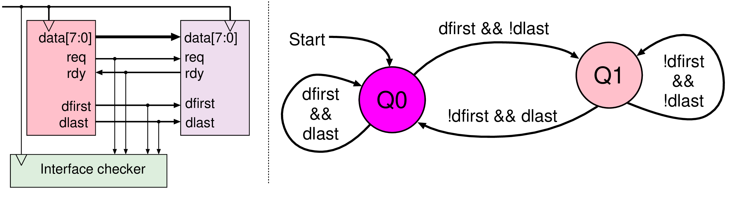
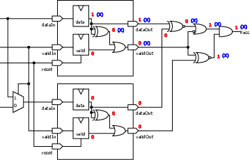
module framed_standard_sync_monitor(
               input reset,
               input clk,           // Clock input. ALL CONNECTIONS ARE INPUTS!
               input req,           // Request signal
               input rdy,           // Ready signal, for the reverse direction
               input [7:0] data,    // Data bus
               input dfirst,        // First word of packet indicator
               input dlast);        // Last word indicator
  bit q1; integer error_flag;
  always @(posedge clk)
    if (reset) q1 = 0;
    else begin
    error_flag = 0;
    if (req && rdy && !q1) begin
      if (dfirst && !dlast) q1 = 1; // Frame start
      else if (dlast && !dfirst) begin
        $display("%m: %1t: C2: End outside of frame.", $time);  error_flag = 2;
        end
      else if (!dlast && !dfirst) begin
        $display("%m: %1t: C3: Byte outside a frame.", $time); error_flag = 3;
        end
    end
    else if (req && rdy && q1) begin
       if (!dfirst && dlast) q1 = 0; // Frame end
       else if (dlast && dlast) begin
         $display("%m: %1t: C1b: One-word frame during existing frame.", $time); error_flag = 1;
         end
      else if (!dlast && dfirst) begin
         $display("%m: %1t: C1a: Frame start during existing frame.", $time); error_flag = 1;
         end
      end
   end
endmodule
  wire en = req && rdy;

  // The transition from Q0 -> Q1 -> ... -> Q1 -> Q0:
  sva_transaction: assert property (@(posedge clk)
    ( (en && dfirst && !dlast) |=> (!en || (!dfirst && !dlast))[*0:$] ##0 (en && !dfirst && dlast) ) )

  // Forbid any exit from Q0 except with dfirst:
  good_Q0: assert property (@(posedge clk)
    ( (en && dlast) || reset |=> (!(en && dfirst))[*0:$] ##0 (en && dfirst) ) )


| Profile | Channels | Other nets | Description |
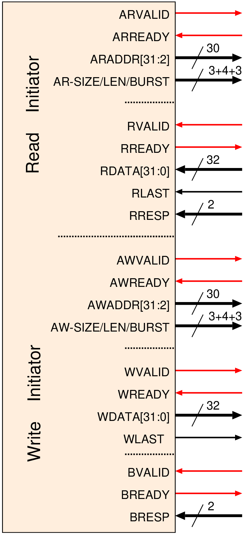
| AXI3 | AR+R, AW+W+B | Tag ID, WLanes | Bursts 1–16 beats |
| AXI4 | AR+R, AW+W+B | Tag ID, WLanes, QoS | Bursts 1–256 beats |
| AXI4-Lite | AR+R, AW+W+B | No burst transfers. No byte lanes |
|
| AXI4-Stream | W | Simplex. No addressing. Unrestricted length |
|
| AXI ACE | All of AXI4 | AC+CR+CD | Cache coherency extensions |
| ACE5-Lite | All of AXI4 | AC+CR+CD | Single beat. Out-of-order responses |


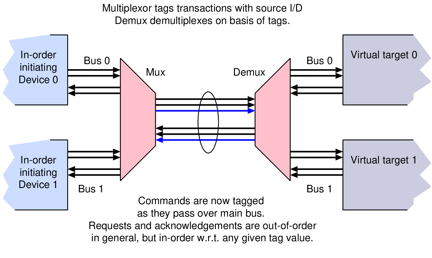
1Profiles:
2    t0: { src: u_M0, type: readRequest, avg: 10, peak: 100, req_beats: 1,
3          resp_beats: 4, qos: 0, lc: false, dst: u_S0 }
4    t1: { src: u_M0, type: writeRequest, avg: 10, peak: 94.3, req_beats: 4,
5          resp_beats: 1, qos: 0, lc: false, dst: u_S0 }
6Dependencies:
7    # Receipt of readRequest at u_S0, triggers a transaction at u_M0
8    d0: { from: u_S0.readRequest, to: u_M0.readRequest }
9


| No. | Name | Description |
| 1. | Rate:
open
loop
| Average rate injection from all ingress ports to all egress ports of 8 byte payloads, with no burstiness |
| 2. | Rate:
open
loop
| Average rate injection from all ingress ports to one egress port, with no burstiness. |
| 3. | Rate:
saturated
| Injection at peak capacity from all ingress ports to all egress ports, with no burstiness. |
| 4. | Rate:
open
loop
| Average injection rate with random delays between injections, from all ingress ports to all egress ports. |
| 5. | Rate:
open
loop
| Average injection rate from all ingress ports to all egress ports, with variable length packets. |
| 6. | Rate:
closed
loop
| Ingress port only generates a new message after previous response. All packets are long (32 bytes). |

|
|
|
|


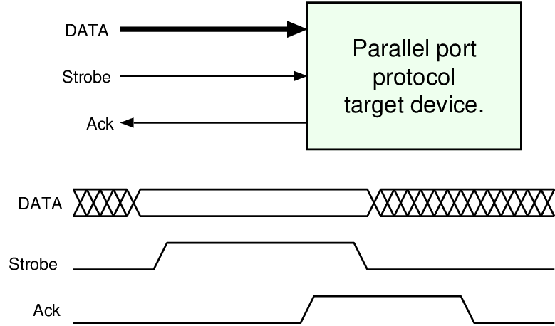
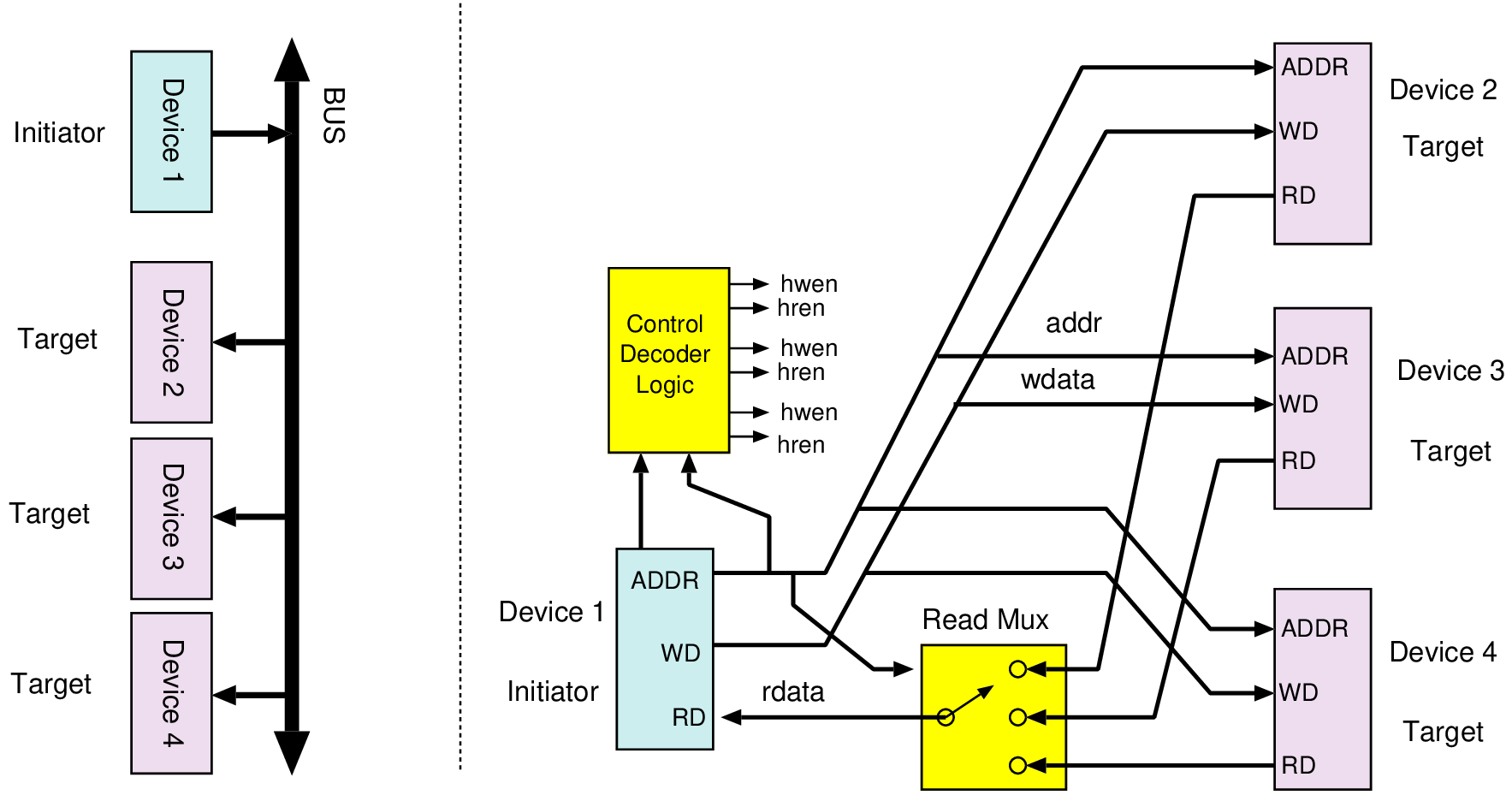
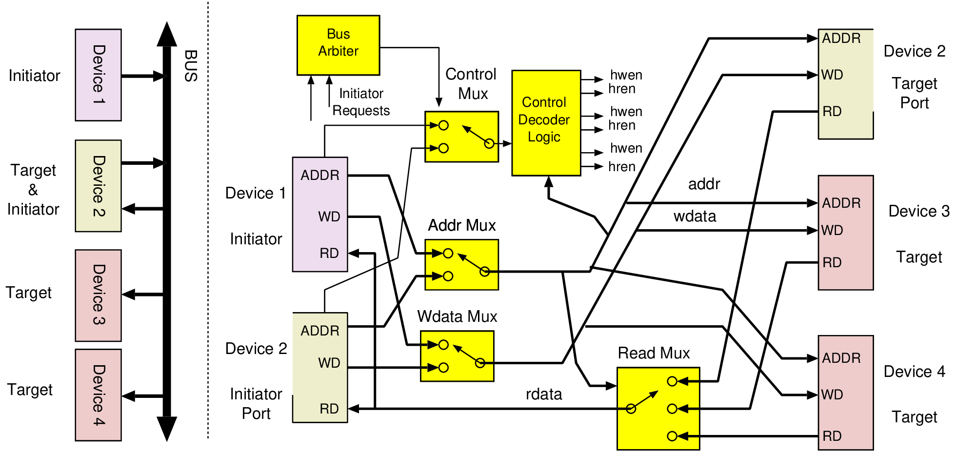
| Connection | Direction | Use |
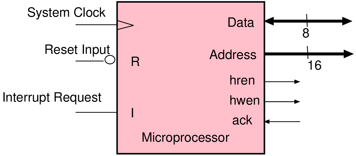
| data[7:0] | I/O | Bidirectional data bus |
| addr[15:0] | Output | Selection of internal address; not all 32 bits are used |
| hren | Output | Asserted during a data read from the target to the host |
| hwen | Output | Asserted during a write of data from the host to the target |
| ack | Input | Asserted when the addressed device has completed its operation |
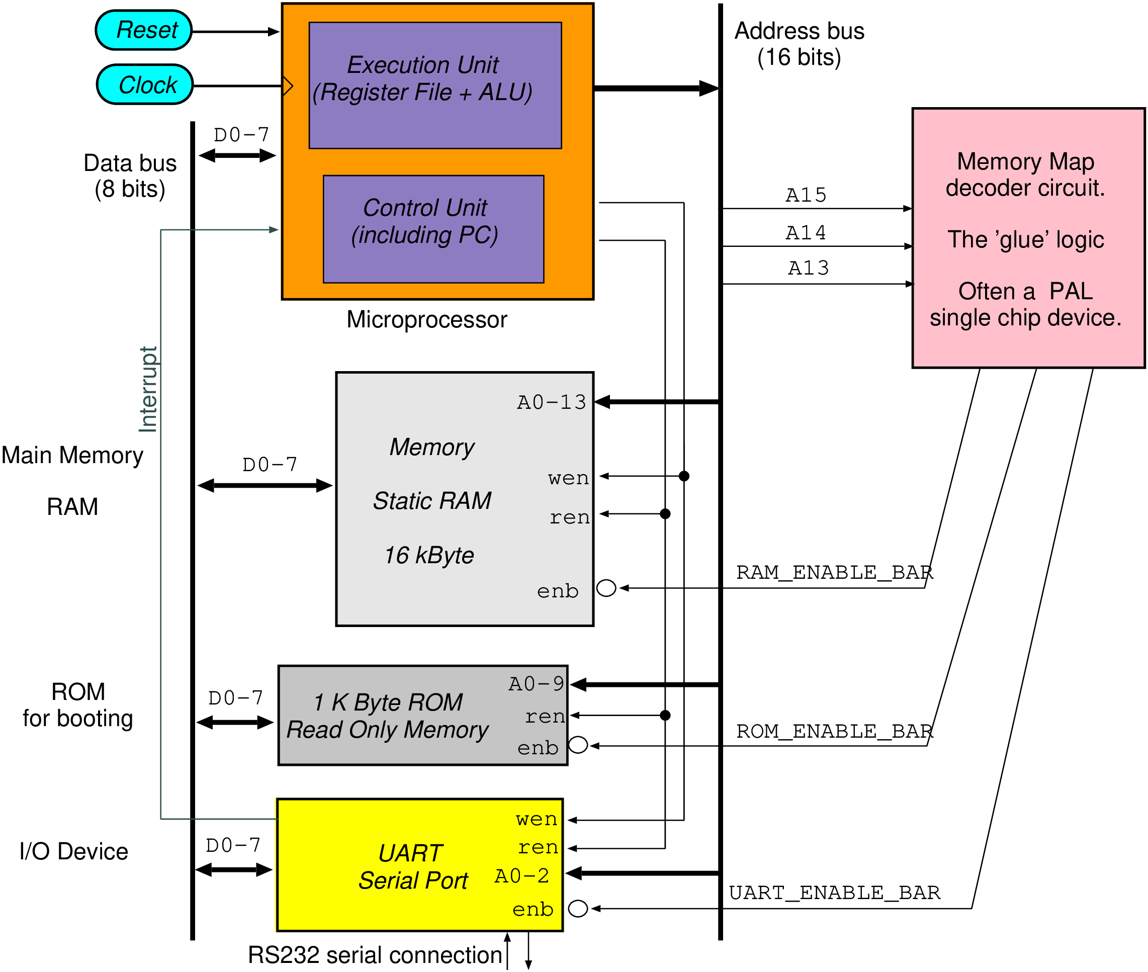
| Start | End | Resource |
| 0000 | 03FF | ROM (1 kbytes) |
| 0400 | 3FFF | Unused images of ROM |
| 4000 | 7FFF | RAM (16 kbytes) |
| 8000 | BFFF | Unused |
| C000 | C007 | Registers (8) in the UART |
| C008 | FFFF | Unused images of the UART |
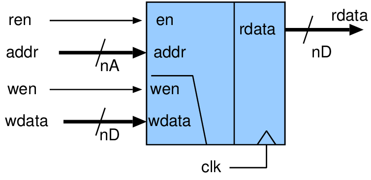
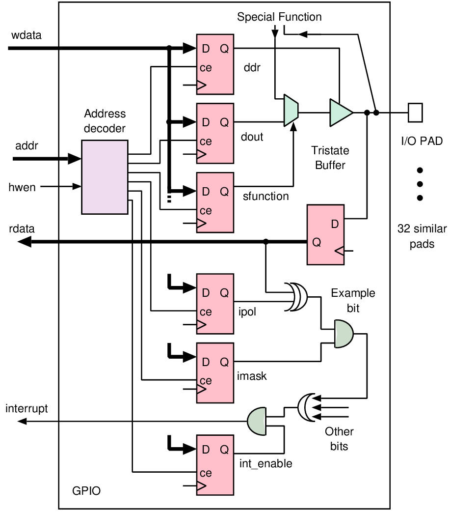
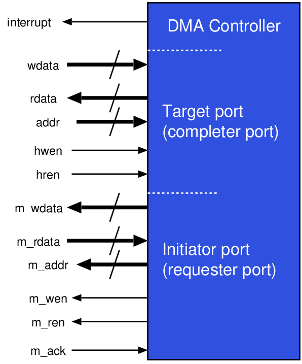
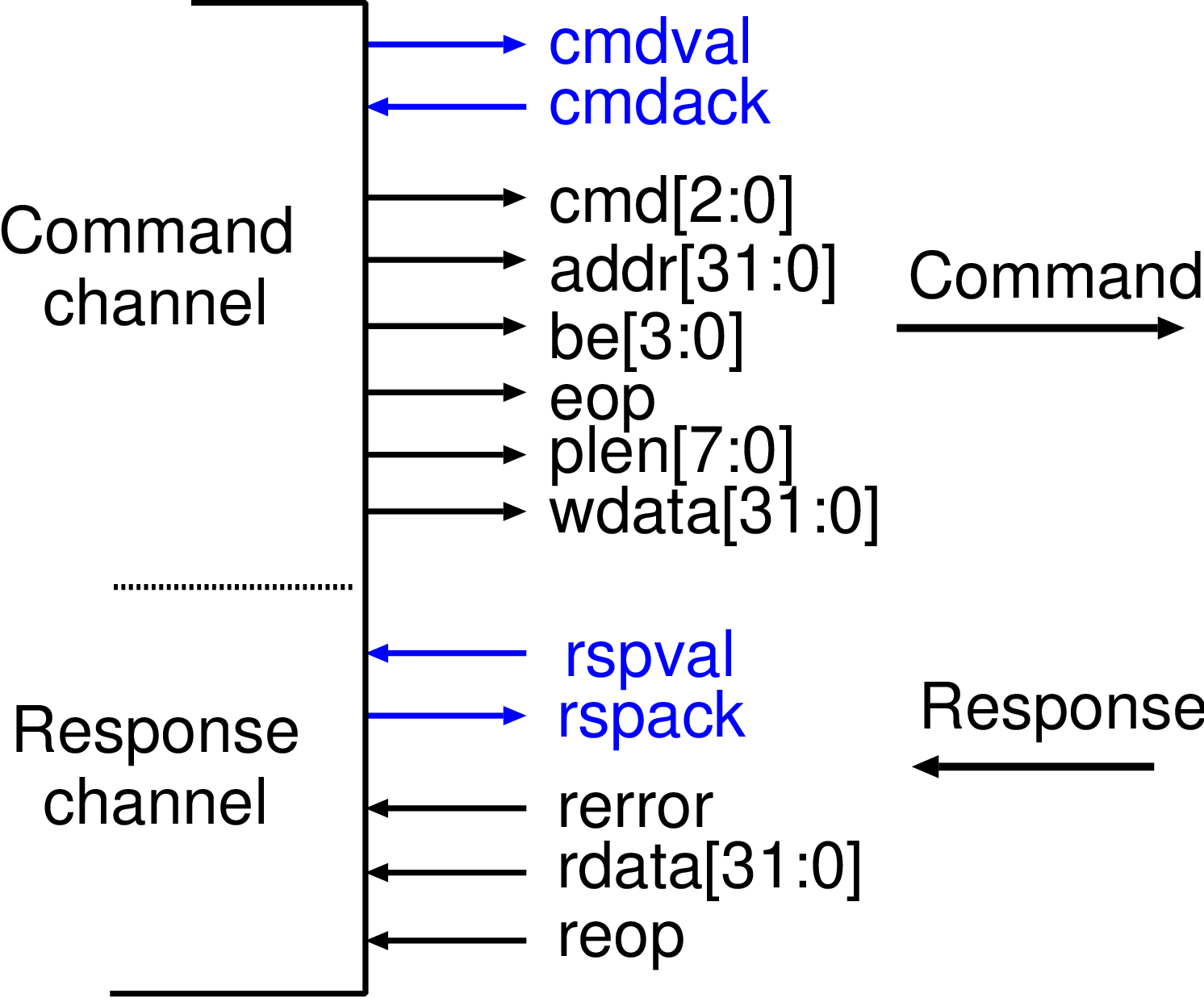
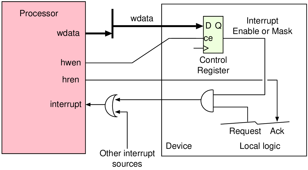
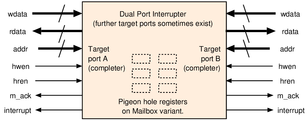
| Connection | Direction | Use |
| addr[31:0] | Output | Selection of internal address; not all 32 bits are used |
| hwen | Input | Asserted during a write from the host to the target |
| hren | Input | Asserted during a read from the target to the host |
| wdata[31:0] | Input | Data to a target when writing or storing |
| rdata[31:0] | Output | Data read from a target when reading or loading |
| interrupt | Output | Asserted by target when needing attention |


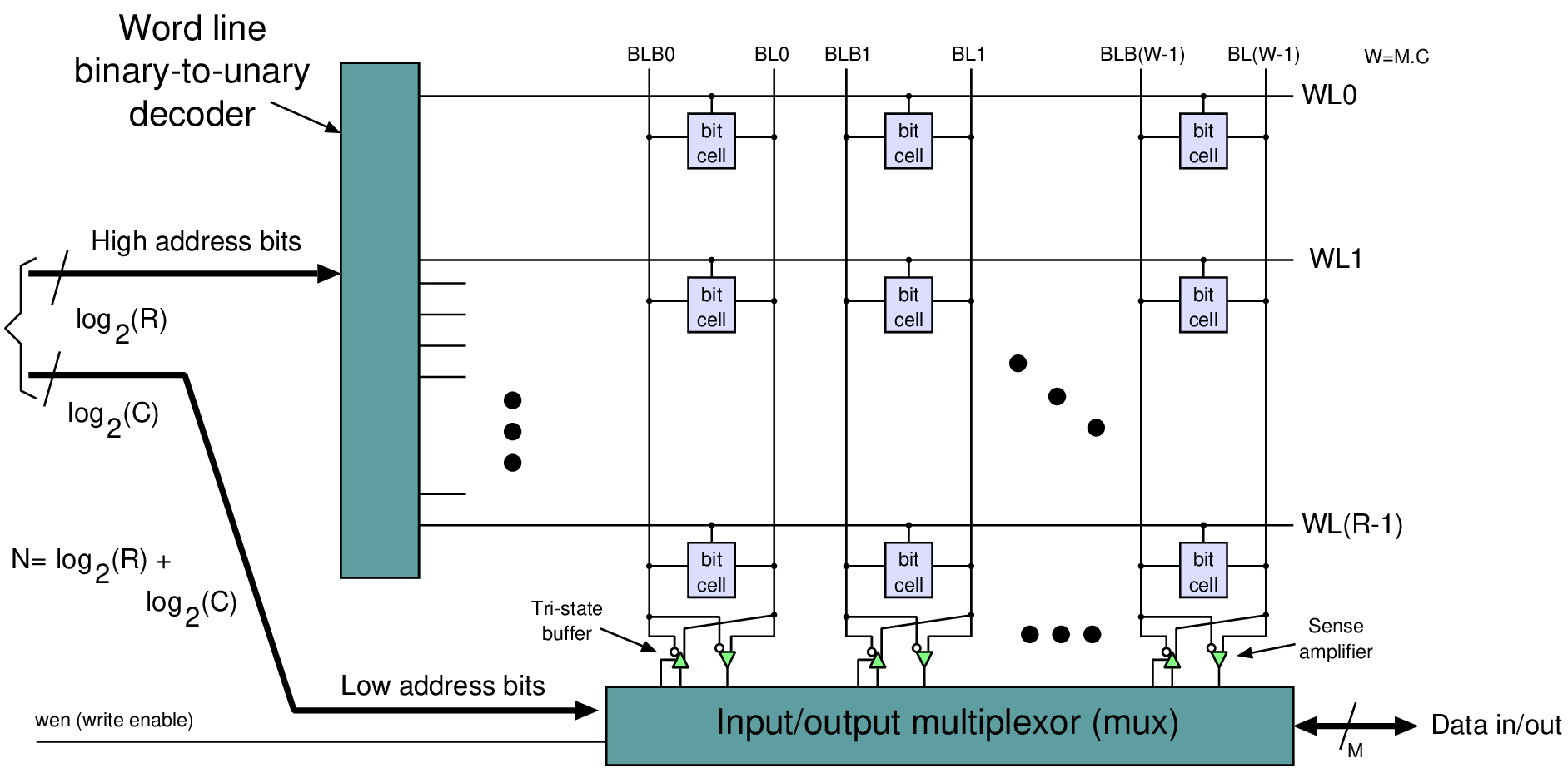
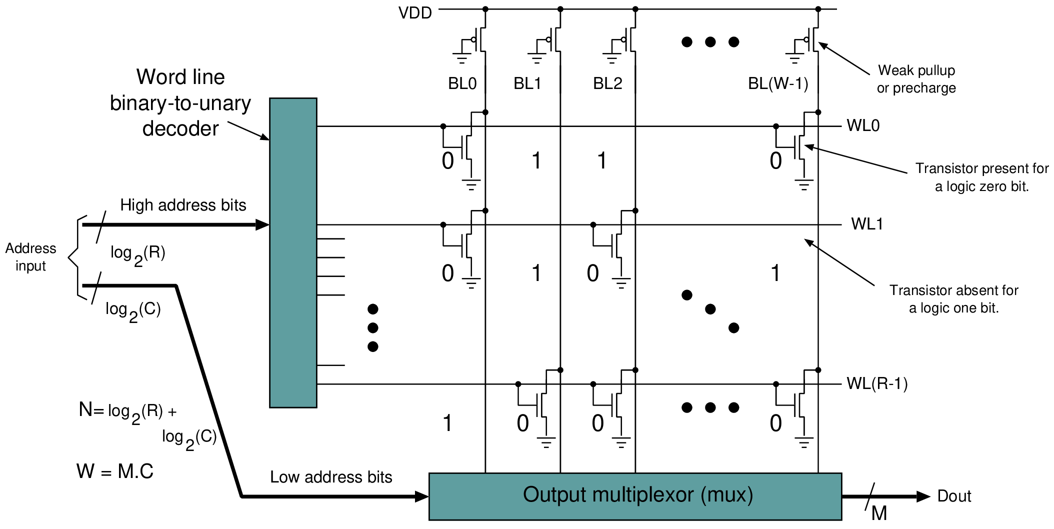
| Memory | Volatile | Main applications | Implementation |
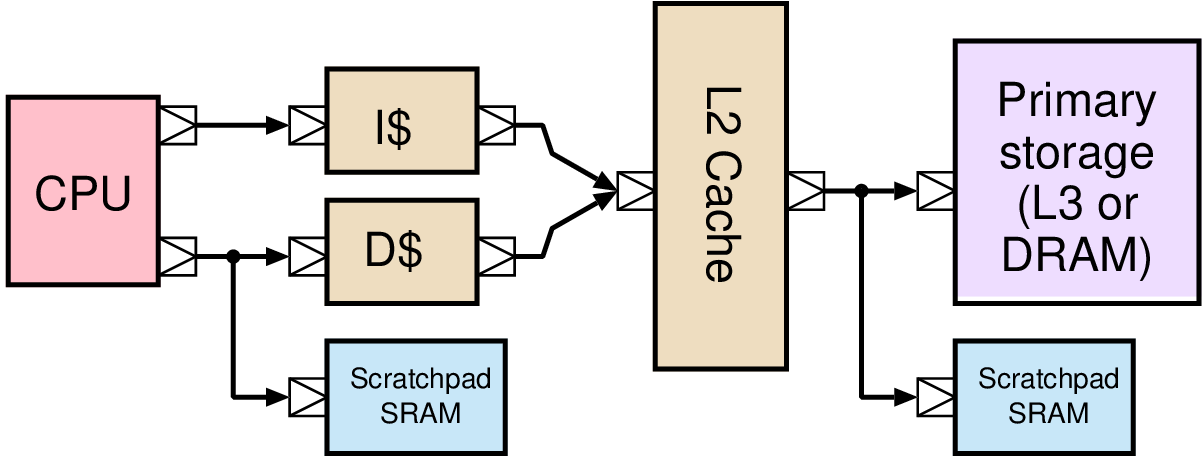
| ROM | No | Booting, coefficients | Content set by a tapeout mask |
| SRAM | Yes | Caches, scratchpads, FIFO buffers | One bistable (invertor pair) per bit |
| DRAM | Yes | Primary storage | Capacitor charge storage |
| EA-ROM | No | Secondary storage | Floating-gate FET charge storage |
| Memristive | No | Next generation | Electrically induced resistance changes |


|
|
|
|
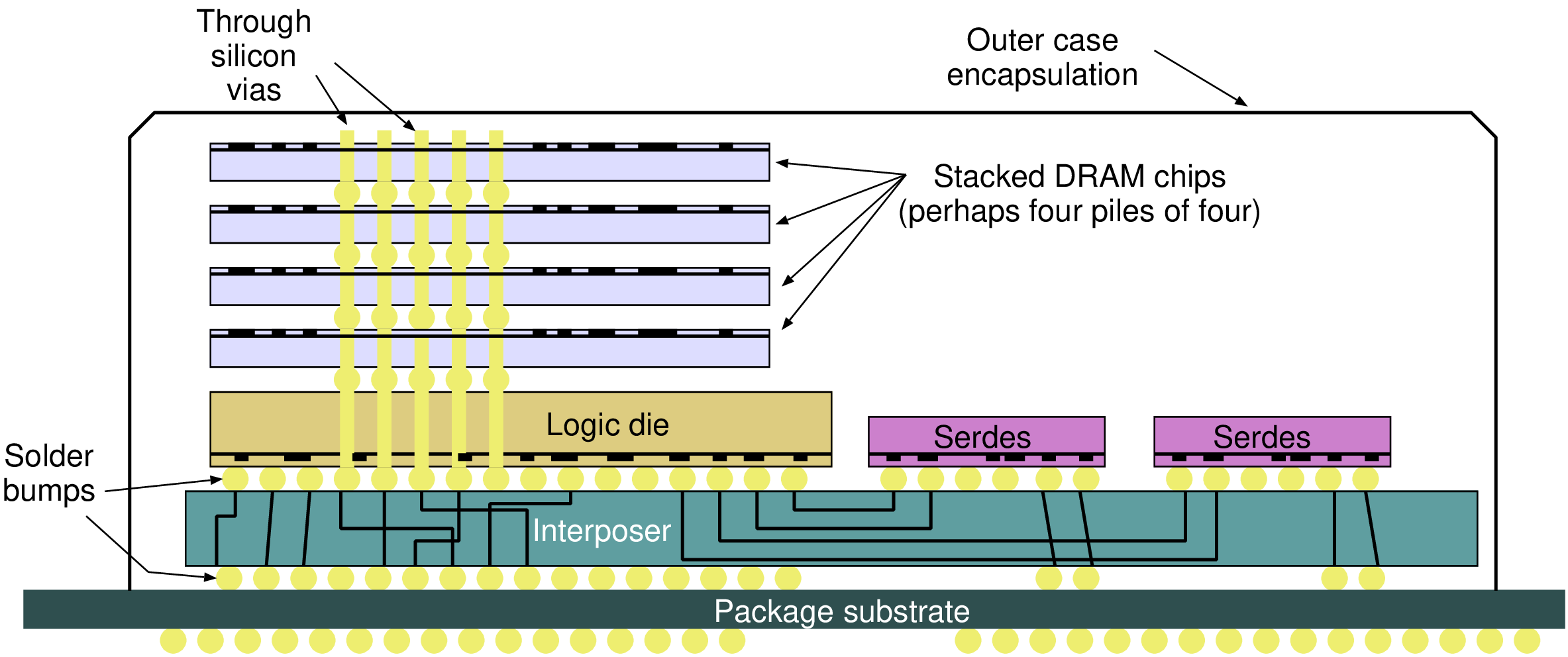
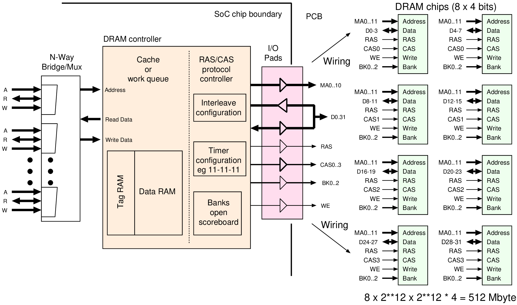
| Quantity | Aggregate capacity | Description |
| 1 channel | 16 GB | A physical bus: 64 data bits, 3 bank bits and 14 address bits |
| 4 DIMMs | 16 GB | Multiple DIMMs are connected on the PCB to one channel |
| 1 rank | 4 GB | A number of logical DIMMs within a physical DIMM |
| 16 chips | | This DIMM uses 16 4-bit chips making a 64-bit word |
| Lanes/chip | 4 bit lanes = 1 GB | Each chip serves a word 4 bits wide |
| 8 banks | | Each bank has its own bit-cell arrays (simultaneously open) |
| | 64 Mbit | A page or row is one row of bit cells in an array |
| (Burst) | 8 words = 64 bytes | The unit of transfer over the channel |
| | 16 kbit | The data read/write line to a bit cell |
|
|
|


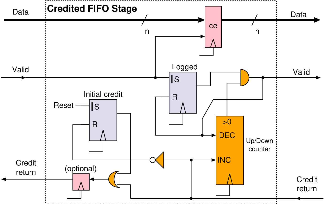
  int burst_tolerance, credit_rate; // Set up by PIO
  int credit;                       // State variable
  void reset() // Complete setup
  { credit = 0;
    register_timer_callback(crediter, credit_rate);
  }
  void crediter() // Called at 1/credit_rate intervals
  { if (credit < burst_tolerance) credit += 1;
  }
  bool police() // Check operation currently allowed
  { if (credit==0) return false;
    credit -= 1;
    return true;
  }

|
|
|

             Thread 1 - Requestor       |           Thread 2 - Server
                                        |
          ...                           |    while(true)
          buffer[1] = operand1;         |    {
          buffer[2] = operand2;         |      if (!buffer[0]) { yield(); continue; }
          write_fence();                |      read_fence();
          buffer[0] = COMMAND;          |      handle(buffer);
          ...                           |      buffer[0] = 0;
                                        |    }

|
|
|
 |  |
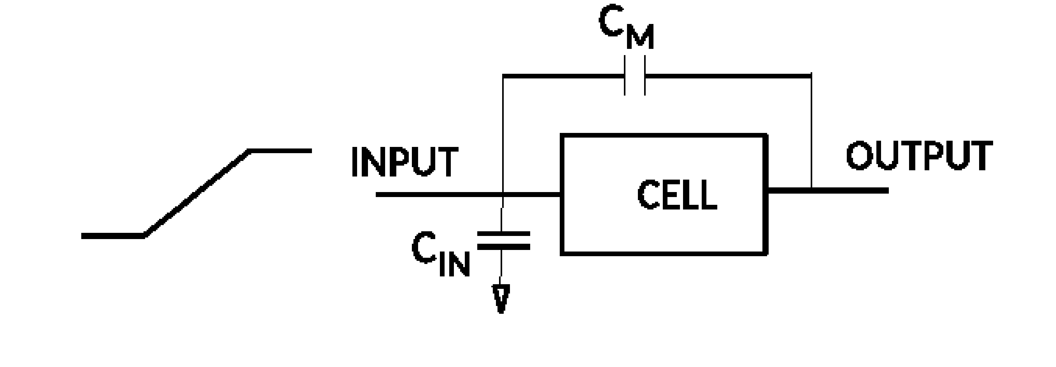
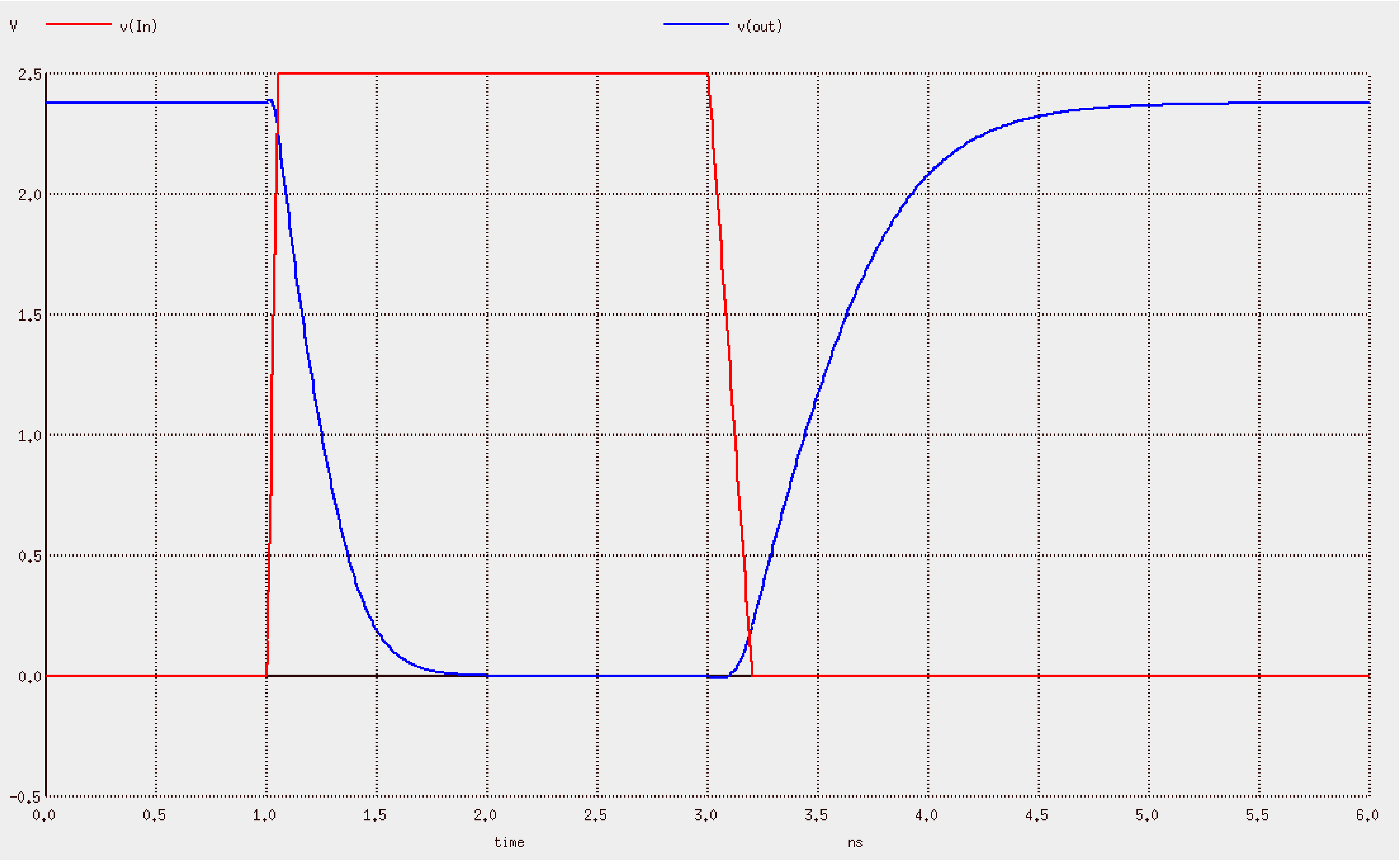
// spice-cmos-inverter-djg-demo.hsp
// Updated 2017 by DJ Greaves
// Based on demo by David Harris harrisd@leland.stanford.edu
// Declare global supply nets and connect them to a constant-voltage supply
.global Vdd Gnd
Vsupply Vdd Gnd DC ‘VddVoltage’
///////////////////////////////////////////
// Set up the transistor geometry by defining lambda
.opt scale=0.35u  * Define lambda // This is half the minimum channel length.
// Set up some typical MOSFET parameters.
//http://www.seas.upenn.edu/~jan/spice/spice.models.html#mosis1.2um

.MODEL CMOSN NMOS LEVEL=3 PHI=0.600000 TOX=2.1200E-08 XJ=0.200000U
    +TPG=1 VTO=0.7860 DELTA=6.9670E-01 LD=1.6470E-07 KP=9.6379E-05
    +UO=591.7 THETA=8.1220E-02 RSH=8.5450E+01 GAMMA=0.5863
    +NSUB=2.7470E+16 NFS=1.98E+12 VMAX=1.7330E+05 ETA=4.3680E-02
    +KAPPA=1.3960E-01 CGDO=4.0241E-10 CGSO=4.0241E-10
    +CGBO=3.6144E-10 CJ=3.8541E-04 MJ=1.1854 CJSW=1.3940E-10
    +MJSW=0.125195 PB=0.800000

.MODEL CMOSP PMOS LEVEL=3 PHI=0.600000 TOX=2.1200E-08 XJ=0.200000U
    +TPG=-1 VTO=-0.9056 DELTA=1.5200E+00 LD=2.2000E-08 KP=2.9352E-05
    +UO=180.2 THETA=1.2480E-01 RSH=1.0470E+02 GAMMA=0.4863
    +NSUB=1.8900E+16 NFS=3.46E+12 VMAX=3.7320E+05 ETA=1.6410E-01
    +KAPPA=9.6940E+00 CGDO=5.3752E-11 CGSO=5.3752E-11
    +CGBO=3.3650E-10 CJ=4.8447E-04 MJ=0.5027 CJSW=1.6457E-10
    +MJSW=0.217168 PB=0.850000
/////////////////////////////////////////////
// Define the invertor, made of two MOSFETs as usual, using a subcircuit.
.subckt myinv In Out N=8 P=16 // Assumes 5 lambda of diffusion on the source/drain
m1 Out In Gnd Gnd CMOSN l=2 w=N
+ as=‘5*N’ ad=‘5*N’
+ ps=‘N+10’ pd=‘N+10’
m2 Out In Vdd Vdd CMOSP l=2 w=P
+ as=‘5*P’ ad=‘5*P’
+ ps=‘P+10’ pd=‘P+10’
.ends myinv

//////////////////////////////////////////////
// Top-level simulation net list
//  One instance of my invertor and a load capacitor
x1 In Out  myinv         // Invertor
C1 Out Gnd 0.1pF         // Load capacitor
//////////////////////////////////////////////
// Stimulus: Create a waveform generator to drive In
// Use a  "Piecewise linear source"  PWL that takes a list of time/voltage pairs.
Vstim In Gnd PWL(0 0 1ns 0   1.05ns ‘VddVoltage’   3ns VddVoltage    3.2ns 0)
//////////////////////////////////////////////
// Invoke transient simulation (that itself will first find a steady state)
.tran .01ns 6ns // Set the time step and total duration
.plot TRAN v(In) v(Out)
.end
 |  |
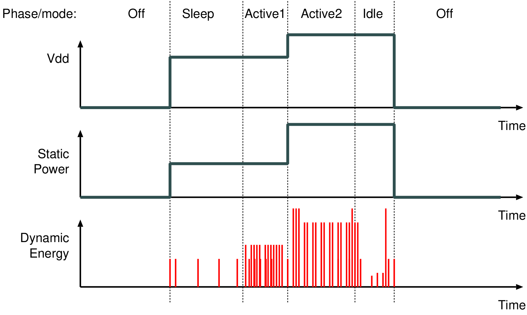
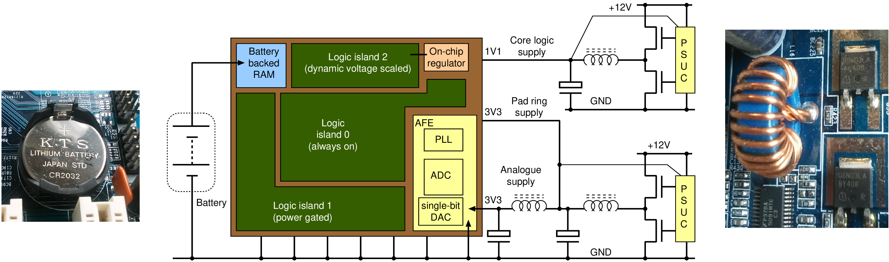
| Clock | Power | |
| On/Off | Clock gating | Power supply gating |
| Variable | Dynamic frequency scaling (DFS) | Dynamic voltage scaling (DVS) |
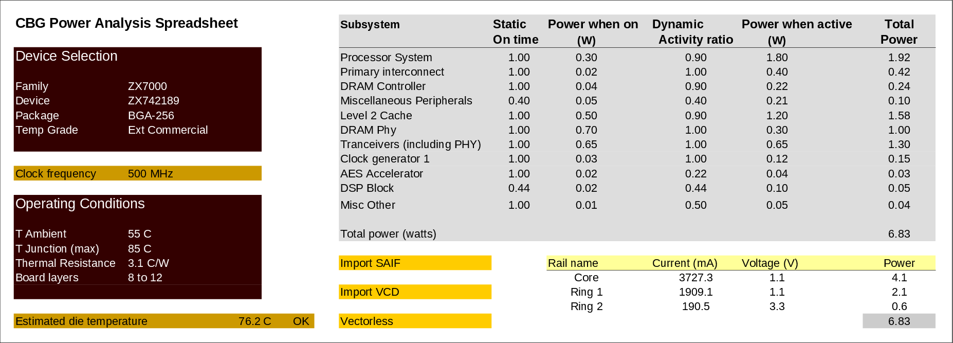
| Supply voltage | Clock frequency | Static power | Dynamic power | Total power |
| (V) | (MHz) | (mW) | (mW) | (mW) |
| 0.8 | 100 | 40 | 24 | 64 |
| 1.35 | 100 | 67 | 68 | 135 |
| 1.35 | 200 | 67 | 136 | 204 |
| 1.8 | 100 | 90 | 121 | 211 |
| 1.8 | 200 | 90 | 243 | 333 |
| 1.8 | 400 | 90 | 486 | 576 |

| Technique | Clock gating | Supply gating | DVFS |
| Control | Automatic | Various | Software |
| Granularity | Register or FSM | Larger blocks | Macroscopic |
| Clock tree | Mostly free runs | Turned off | Slows down |
| Response time | Instant | 2 to 3 cycles | Instant (or ms if PLL adjusted) |
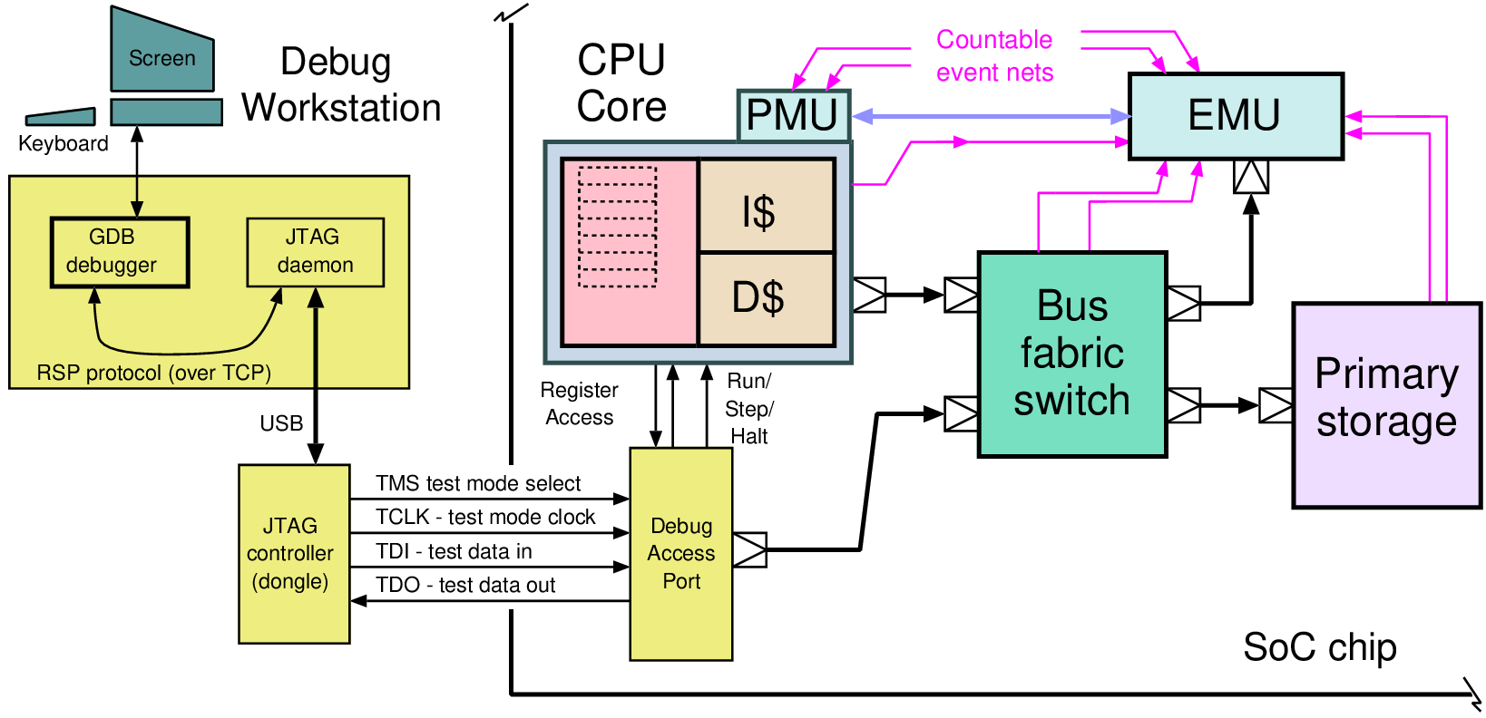

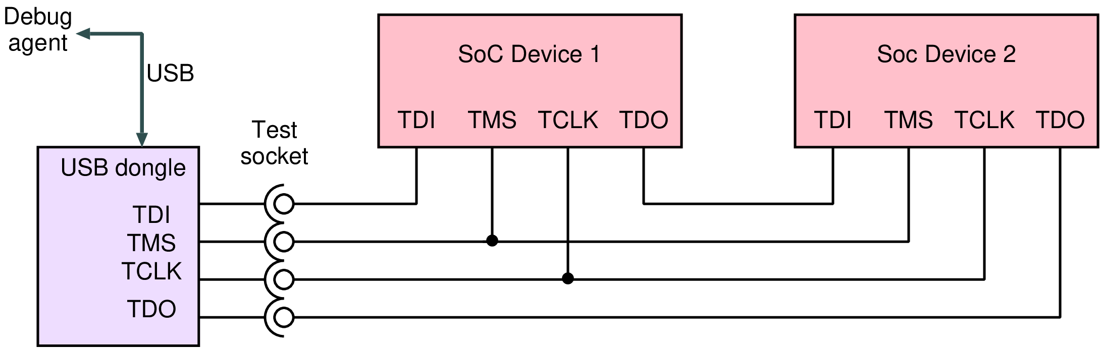
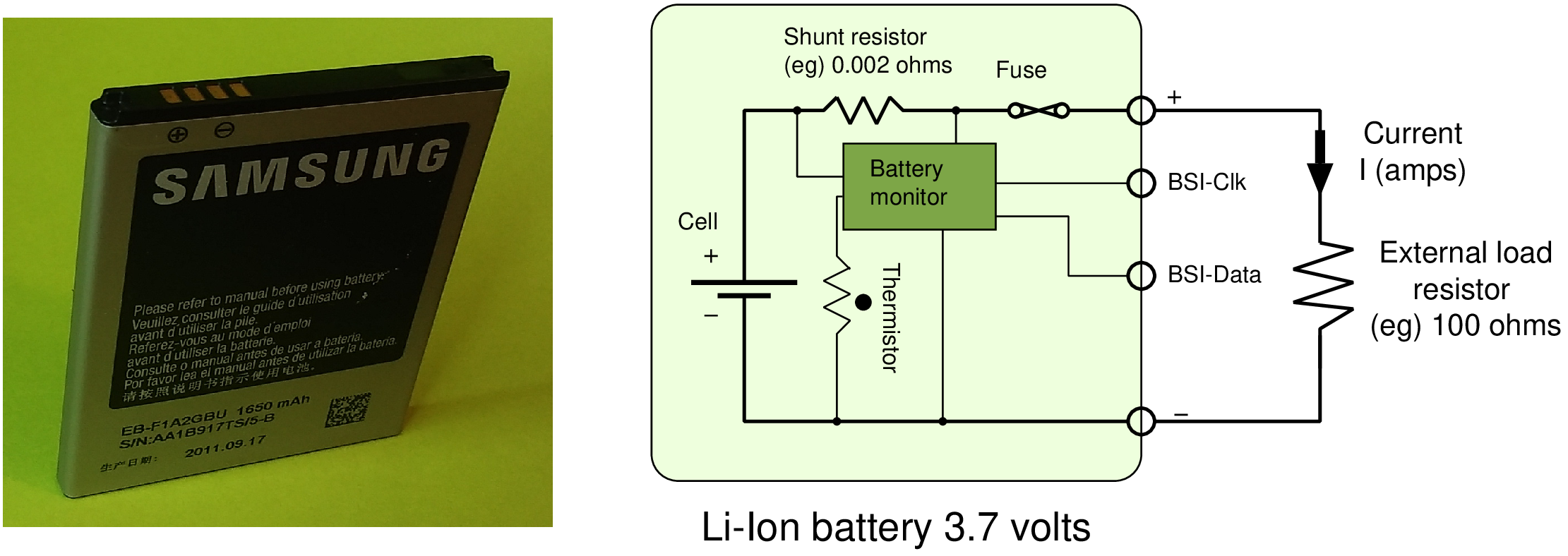
| TDI | In | Test data in: serial bits from test agent or previous device |
| TMS | In | Test mode select: frame data and addresses |
| TCK | In | Test clock: clocks each bit in and out |
| TDO | Out | Test data out: to next device or back to agent |


©2021 - DJ Greaves. All figures are available for use under creative commons CC BY 4, unless otherwise stated.