Computer Hardware: How Computers Work

Dr David Greaves
Corpus Christi College
and
Computer Laboratory
University of Cambridge
We'll look at 'what is a digit', how to make a logic function using electicity and 'what is a computer' and, putting these all together, end up with an electronic digital computer.
Video Versions
A video version of some of this material is available here, but I normally present this material live from the slides lower down on this web page.
You may find that watching the videos at 1.5 times normal speed is a good idea, but pausing and replaying at points of interest.
- 1 (33 mins) Fundamentals of Digital Hardware (digital history and computer structure).
- 2 (15 mins) Electrical Processing of Bits.
- 3a (30 mins) From Ladder Logic to Sequential Circuits.
- 3b/c (25+35 mins) Computer Memory Hardware.
- 4 (39 mins) Assembling A Computer and the Fetch/Execute Cycle.
Video 1: Fundamentals of Digital Hardware - Digits and Computer History
The first video (33 minutes or so) has the following five major sections:
- Parts of a modern PC motherboard,
- What is a digit?
- Two example programs: with and without use of main store,
- Computer History - from Babbage to EDSAC,
- Computer basic structure.
Watch video 1 here:
[Errata: 'ome' caption after front panel lights. 'every natural number' not 'very natural number'. Panning of Padua slide.]
Video 2: Electrical Processing of Bits: on/off circuits and one-bit logic.
The second video gives you some basic instruction in
electrical circuits and then looks at how the
telegraph influenced the design of electonic
computers. It looks at how to store individual
bits and introduces basic logic functions using
relays and logic gates.
Watch video 2 here (15 minutes):
Note: Yellow LED is indicator A and Green LED is indicator B. Spring inside the 'relay'at 9:10.
Video 3a: From Ladder Logic to Sequential Circuits.
Computer arithmetic circuits: The third video talks about computer arithmetic and describes how to build some important sub-circuits, such as adders and counters. The content here will all be covered in the CST Part Ia Digital Electronics course.
Watch video 3a here (30 minutes):
Videos 3b and 3c: Computer Memory Hardware
Please proceed directly to video 4, skipping videos 3b and 3c if this is your first visit to the this site.
3b: Computer Memory History and Highlights (34 minutes): Primary vs Secondary Storage, Delay lines, Tapes, Disks, Static RAM, Dynamic RAM, Flash and other semiconductor memories (25 minutes). This includes a 5-minute section on Memory Formal Specification that should certainly be skipped on first viewing.
3c: Internal Structure of Semiconductor Memories. 1-SRAM from transparent latches (the skinny approach). 2-Making a squarer chip. 3-Bit cell designs: A1-SRAM cells, A2-DRAM cells and A3-EAPROM cells - Electronically Alterable Programmable Read-Only Memory (Flash).
Watch videos 3b and 3c here:
|
|
Video 4: Assembling A Computer and the Fetch/Execute Cycle
Video 4 contents:
Watch video 4 here (39 minutes):
Ancillary Video - Basic MOSFET Transistor Operation
The surrounding materials on these web pages mostly use electromechanical relays to illustrate logic circuits.
In reality, most of today's computers use MOSFET transistors, as described in this short, ancillary video.
Perhaps also read Systems Design, 12 Lectures to Part Ia. (PDF, 96 pages)
How Computers Work - Lecture One - Components and Bits
Because computers have not really changed design from John von Neumann's seminal work, or even since the time of Sir Charles Babbage, knowledge of the history of computers is knowledge of today's general purpose computers!
This first lecture looks at the low-level components needed to make a standard computer in any technology.
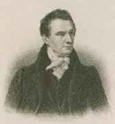
Charles Babbage - The Inventor of the Computer
Born December 26, 1791 in Teignmouth, Devonshire, UK. Died in 1871, London. Known as the 'Father of Computing' for his contributions to the basic design of the computer through his Analytical Machine.
Babbage Difference Engine
A mechanical calculator with FIXED (hardwired) program.
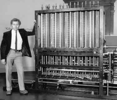
Computers and calculators need storage to keep data.
Computers store their program as well.
Today, storage is in REGISTERS or MAIN MEMORY/STORE, or SECONDARY MEMORY/STORE. The Difference Engine only had registers.
Digital storage stores digits. Babbage used base 10, not binary.
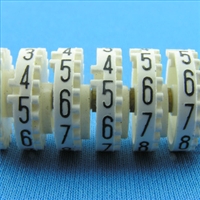
Digital storage mechanisms need to be tolerant to noise: digits must recover from small jogs and move back to one of their nominal settings.

The little white wheels provide what Babbage called the 'carriage' - the means to increment the next-most-significant
digit when a given digit overflows.
In early mechanical designs, there was generally one arithmetic unit (ALU) per register.
Key insight from Babbage: use just one main ALU served by a large, yet simple, data store.
Programming
A program is a list of instructions (a sequence of things to do in the future):
Four basic insruction types: change a register, load/save register from/to main memory, PC change, I/O.
Jacquard Loom
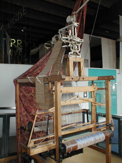
The loom is controlled with punched cards that describe the pattern to be woven.
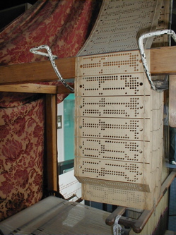
The card under the reader is the current point in the program (program counter or PC).
There is no GOTO statement: the instructions are followed in sequence, but perhaps some could be predicated ?
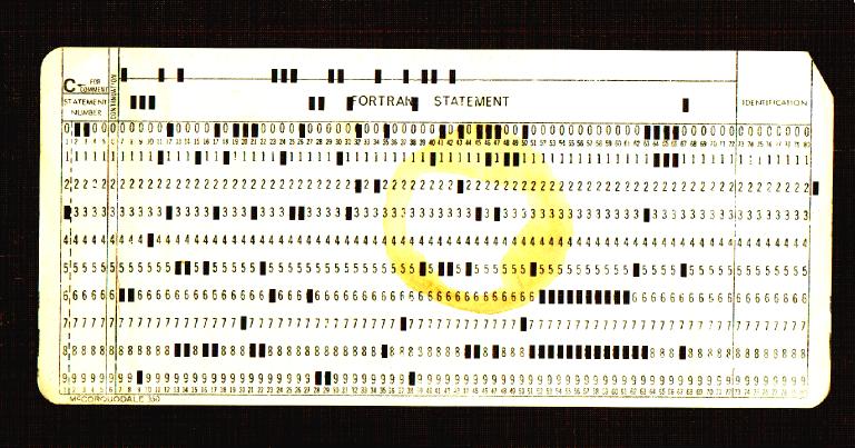
This card reads '300 FACTORIAL PROGRAM BY GREAVES ------ '. No it doesn't, I've lost that one.
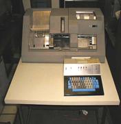
I created it using a sort of typewriter like this IBM 029 Card Punch.
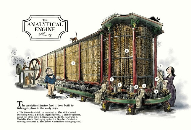
Babbage's Second Design: The Analytical Engine
Babbage realised that having a dedicated adder for every register was overly complex in general (parallel vector processing is a special from that tends to still use this).
He split the machine into:
- the Mill with three registers coupled with adders and other logic (sufficient to do long multipication and long division)
- and the Store of arbitrary size (going off to the right) with a linear array of simple registers for main data storage.
- Punched cards served the program and also could be read and written as secondary storage like today's disk drives and USB memory sticks.

Electronic Era
1947: EDVAC
The EDVAC was an early electronic computer that had separate memories
for program and data. Main memory held 1024 ten-digit decimal numbers.
Stored-Program Computation
John von Neumann - The Second Inventor of the Computer
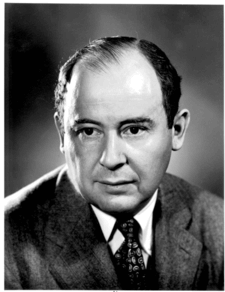
First Draft of a Report on the EDVAC (commonly shortened to First
Draft) was an incomplete 101-page document written by John von
Neumann and distributed on June 30, 1945. Program and data were to be put in the same type of memory.
PDF.
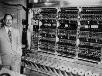
EDSAC: A stored-program computer.
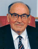
Prof Sir Maurice Wilkes,
University of Cambridge, Computer Laboratory:
EDSAC: .jpg)
Electronic Delay Storage Automatic Calculator (EDSAC) was an early British computer. The machine, having been inspired by John von Neumann's seminal First Draft of a Report on the EDVAC, was constructed by Maurice Wilkes and his team at the University of Cambridge Mathematical Laboratory in England. EDSAC was the first practical stored-program electronic computer.
A smaller machine was built in Manchester by Alan Turing and his team. Both groups had secretly worked on code-breaking machines during the Wold War II.
Alan Turing: 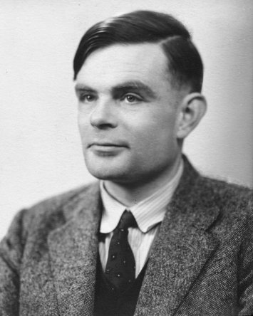
EDSAC was supported by J. Lyons & Co. Ltd., a British firm, who were rewarded with the first commercially-applied computer, LEO I, based on the EDSAC design. EDSAC ran its first programs on May 6, 1949, calculating a table of squares and a list of prime numbers.
EDSAC could address 1024 main memory locations, although only 512 were initially implemented. Each contained 18 binary digits.
Since then, really the only developments have been speed, size, electricity used and storage capacity: the
design has not changed!.
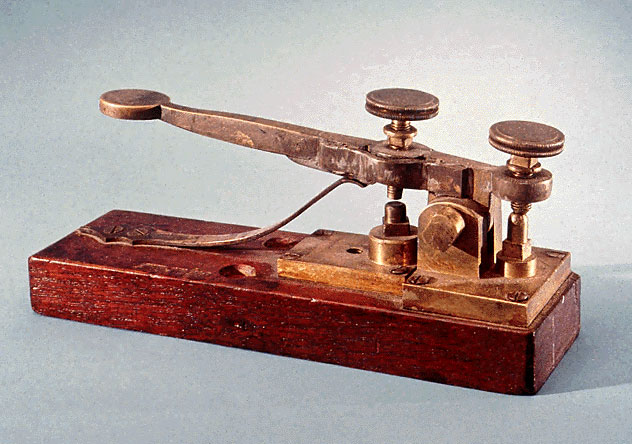
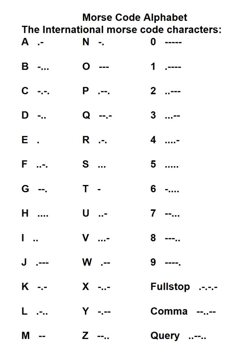
Electronic Computing Basics: The Telegraph
Morse Code
Morse code tapper used for sending a telegram.
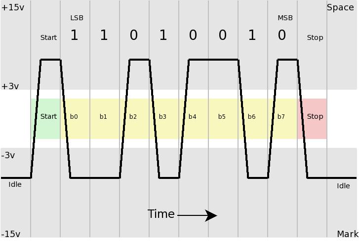
Serial and Parallel Communication
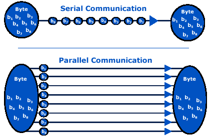
With eight wires, using binary on each line, you can send one BYTE at a time.
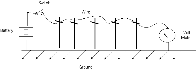
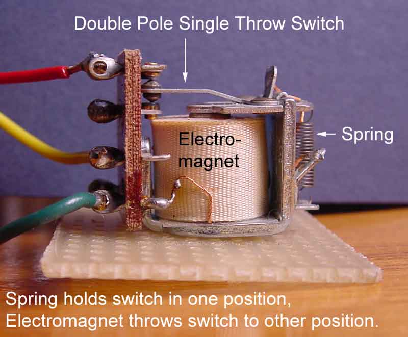
A Relay Station
Wire degrades the signal. Need a human or electro-mechanical relay every 50 or so miles.
An electro-mechanical relay is a switch operated by an electro-magnet.
It keeps our binary digits clean.
Buffering (relaying) the telegraph signal:
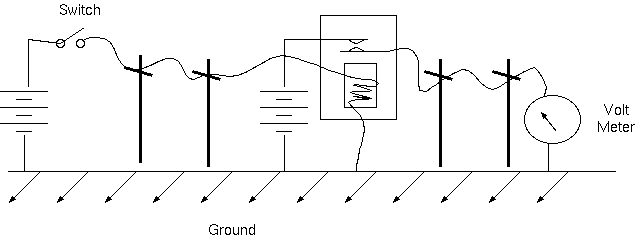
Viewing it as a logic circuit.
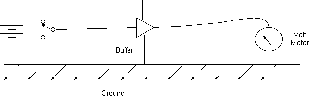
Rather than many miles, the same ideas are used for sending
information a few centimetres over a circuit board or
a fraction of a millimetre over a silicon chip. We then need only one battery or power supply.
Mechanical Teletype: Advantages: don't need to learn Morse Code, don't need to manually write it down at the receiving station, faster.
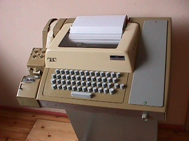
Modern character set:
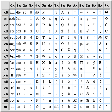
Use an 8-bit byte for each character sent.
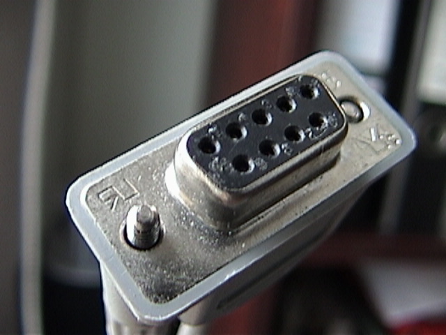
Compatibility: You can still plug a 1950 mechanical teletype into a recent laptop using the RS-232 serial port.
Only one wire in each direction is actually needed: so with a ground (earth reference) connection as well, a total of three pins are commonly used on the nine-pin serial connector.
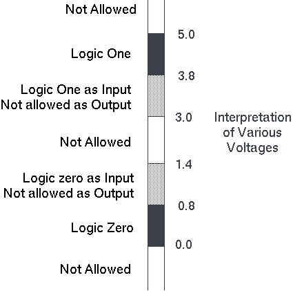
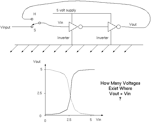
Gate Transfer Curves: Keep those digits clean!
Plots of input and output voltage for the basic components.
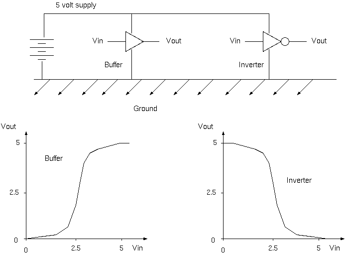
Characteristic shape: flat at the edges, sharply changing in the middle: keeps binary digits clean.
Voltage meanings and margins (five volt system):
How To Store One Bit Electrically
Electro-mechanical implementation: Using a relay
A latching-relay can hold one binary digit (one bit): it is a bi-stable or flip-flop. 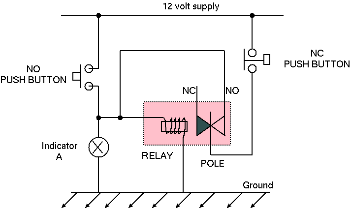
Alternative Implementation: Electronic
Flip-flops made from two inverters in a ring are the main means of making registers in silicon chips today.
The mechanical and electronic bistables are both volatile, meaning that information is lost when the power is removed.
Speed of switching: relay is at least a million times slower than a transistor.
Size of the switch: relay uses about 100 million times the substrate area.
Besides bistables, most computers today store data as magnetic
spots on the hard disk and static electricity charges in Flash and DRAM memories. These give a few orders of magnitude greater
density than transistor bi-stables.
A Logic Gate
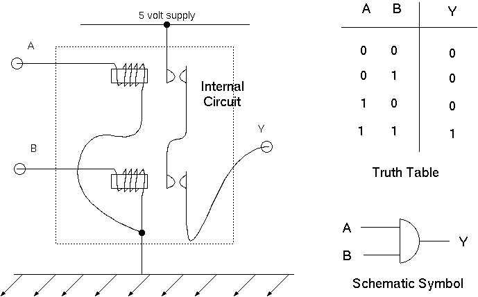
The simplest function we can compute is implemented by a basic logic gate.
My logic gate is implemented with two relays: while they are both activated
by logic ones on their inputs, the output becomes a logic one.
On silicon chips, gates are made out of field-effect transistors and four transistors
are used instead of two relays.
Other Basic Gates
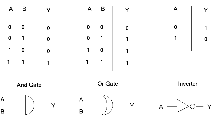
There is also an XOR gate, and versions of AND and OR with inverted outputs
called NAND and NOR.
Adder Circuits
A half adder tallies two inputs creating a binary number in the range 0 to 2.
    A  B  |   C  S
    --------------
    0  0  |   0  0
    0  1  |   0  1
    1  0  |   0  1
    1  1  |   1  0
|
The full adder: made of two half adders:
A full-adder tallies three inputs creating a binary number in the range 0 to 3.
A full-adder tattoo: 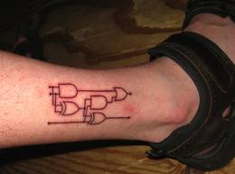
Larger adders can be made by cascading full adders:
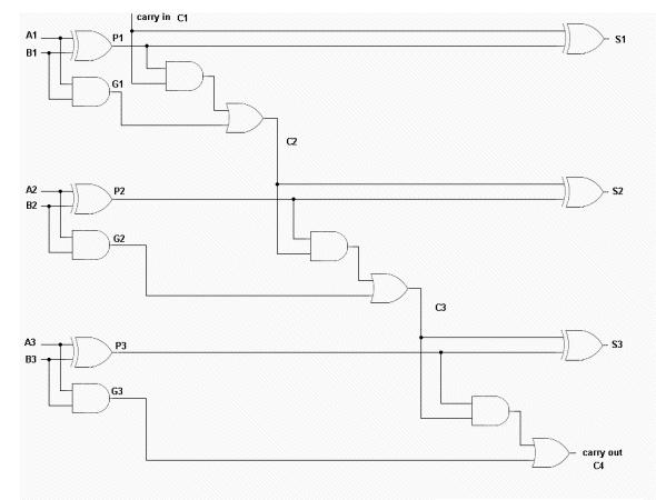
A three bit-adder is made from three full adders (six half adders).
A3 A2 A1 B3 B2 B1 | C4 S3 S2 S1 ------------------------------------- 1 0 1 0 1 0 | 0 1 1 1 5 + 2 = 7 |
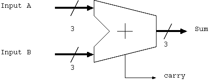
Three-bit adder schematic symbol (hides the details):
Gate count: each gate is roughly 4 transistors. A three bit adders is 15 gates = 60 transistors.
Moore's Law

Moore's law describes an important trend in the history of computer hardware: that the number of transistors that can be inexpensively placed on an integrated circuit is increasing exponentially, doubling approximately every two years. The observation was first made by Intel co-founder Gordon E. Moore in a 1965 paper.
The largest chips are about the size of a fingernail.
There are five or six major chips in a Nintendo DS, and dozens of small ones.
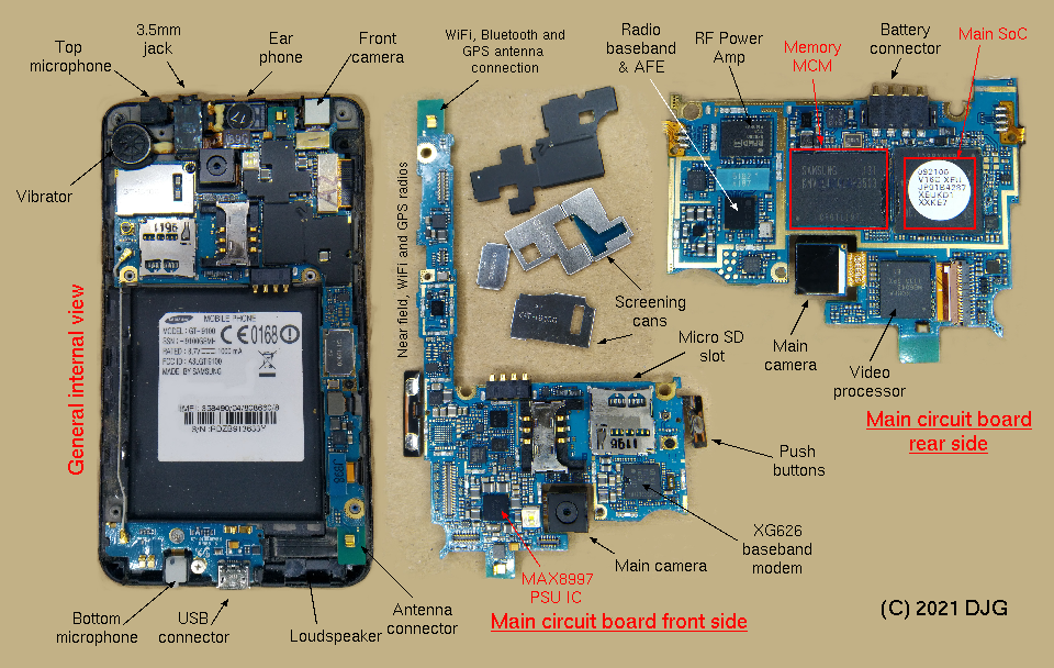
Internal parts of a smart phone (from
Modern SoC Design on ARM by DJ Greaves (P) 2021);
full text (local access only) LINK).
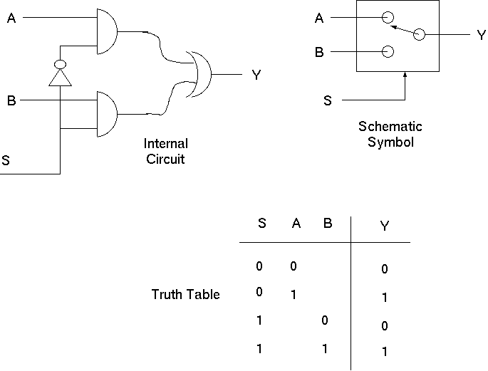
Multiplexor: Another Basic Component
Making a transparent latch flip-flop
![]()
Putting flip-flops together to make a register.
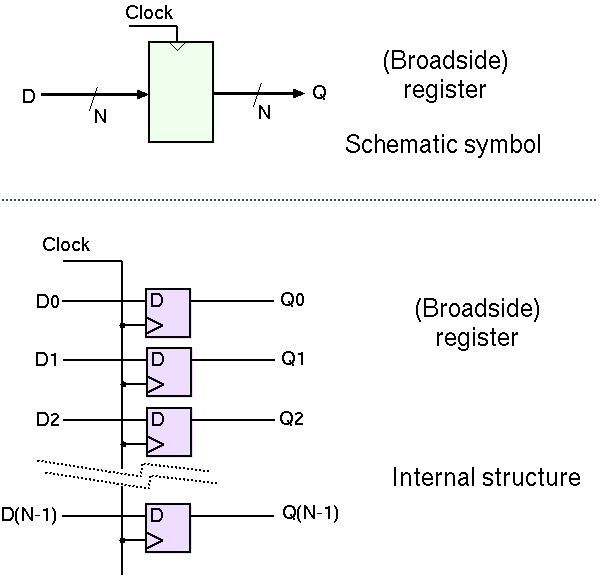
(These flip-flops are edge-triggered, meaning that they sample
their input data on the positive edge of the clock. Internally, they
use a pair of transparent latches).
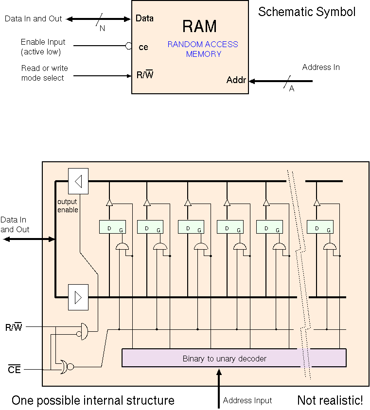
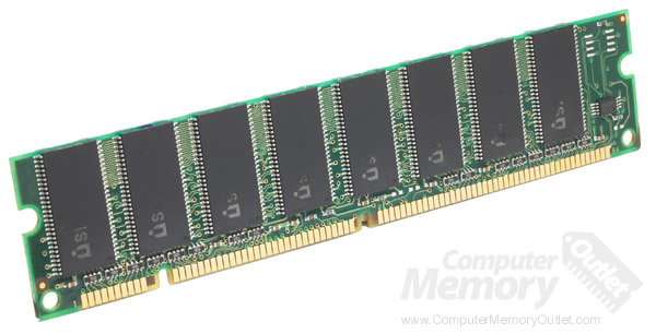
Primary Storage/Main Memory: RAM - Random Access Memory
Possible implementation of RAM using a linear array of registers:
Dynamic RAM
Larger arrays are made using dynamic technology, using electric charge on a capacitor to store a bit instead of the ring-pair of inverters: .
Other important components: Counter and Clock
The clock generates a regular series of transitions.
A counter increments on each clock pulse.
How to make a counter from an adder and a broadside register:
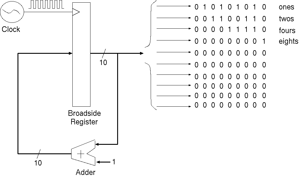
With ten output wires, the count range is 0 to 4095.
Schematic symbol hides the details: 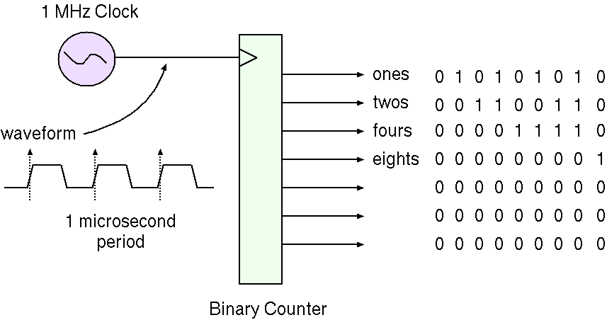 .
.
How Computers Work - Lecture Two - We Now Have Sufficient Components to Build a Complete Computer
Come back and look at these slides in your own time ... or
perhaps study the Little Man Computer
or perhaps Nand To Tetris: The Elements of Computing Systems / Nisan & Schocken
www.nand2tetris.org"
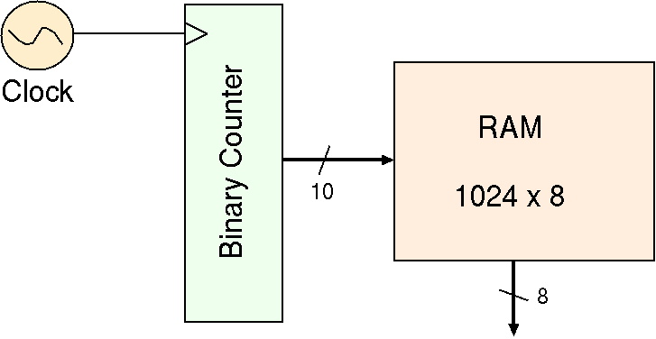
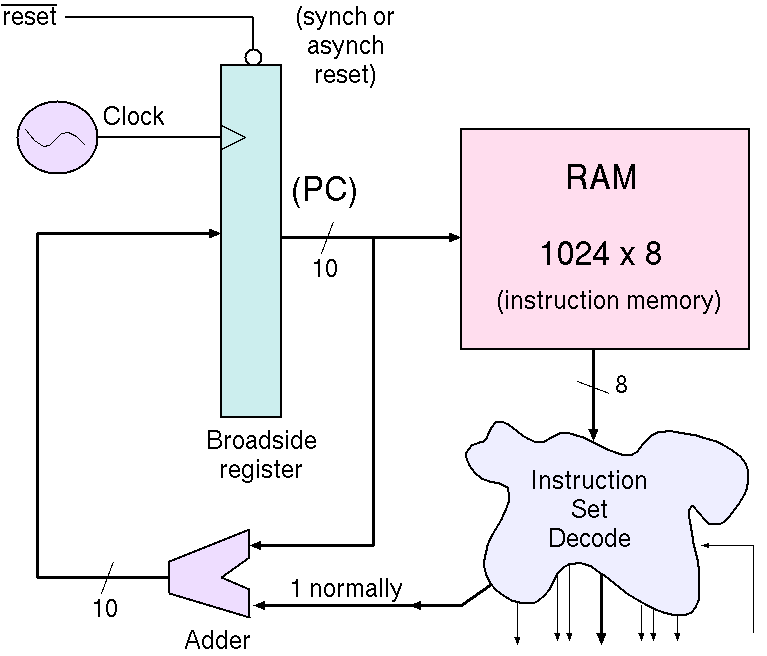
The counter output can index a RAM containing instructions.
Put instructions in the RAM and it steps through them in sequence, like stepping through the Jacquard punch cards.
Here we add a multiplexor between the adder and the broadside register.
This enables a new value to be seeded.
One of the instructions can be a GOTO, that operates the multiplexor
to select a branch destination.
The ALU is an arithmetic and logic unit: it can compute a variety of functions
of its two inputs.
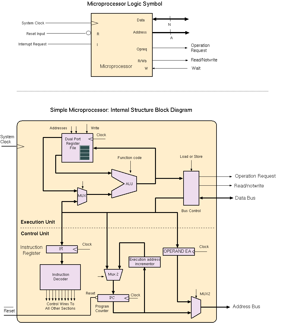
The combination of control and execution units on a single chip
is a called a microprocessor.
[When there are several of these on a chip, each pair of them is
called a core and the core also typically has its own small cache.]
A single bus connects the processor to the memory system. This has
been called the von-Neumann bottleneck. It is avoided in today's computers
by dedicating a large fraction of the processor chip to cache memories.
Having simultaneous access to several caches gives access to instructions and data
in parallel.
(You can do all this using relays if you want: A relay-based computer).
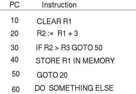
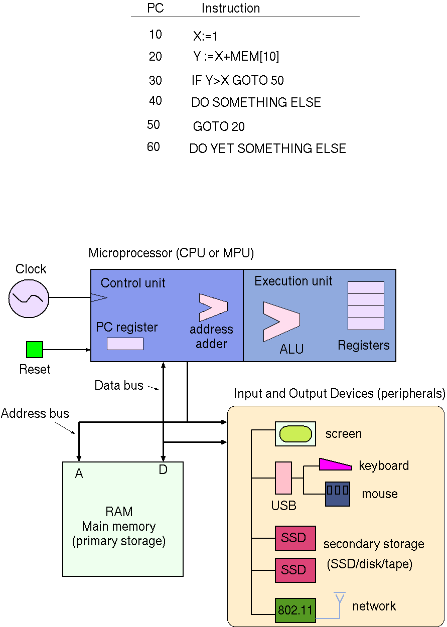
Here is our program again, together with the recap of the blocks found in an everyday (von Neumann) computer:
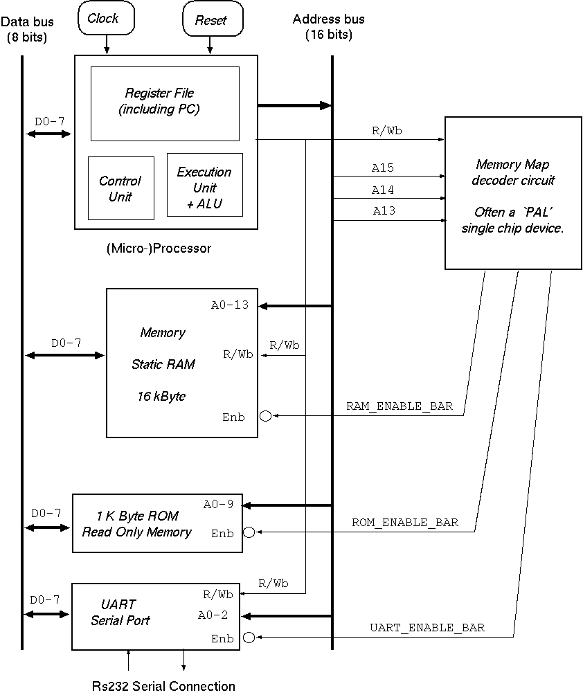
Understanding typical computer bus structures:
Conventional computers cannot be made any smaller or faster out of silicon: we are running out of atoms!
Today's (2014) new computers have multiple conventional computer cores on
one chip: for example the "Intel Core 2 Duo" or the AMD "Turion". The
cores all sharing the same main memory.
Since data movement has become the dominant use of electricity in computers, and the cost of ALU logic has become close
to zero with increasingly smaller transistors, there is also movement back towards the style of Babbage's Difference Engine. In that
design, functionality was hardwired and ALUs were associated with storage locations instead of being centralised in the mill. Custom
processors for social graph processing, AI inference and DNA sequencing are very common (2022).
But the mainstream von Neumann design remains king and we are seeing the number of cores on the processor chip growing. New classes
of algorithms that are better adapted for parallel processing are needed (2022).
But the size of an atom and the speed of light are fixed, so a new approach is needed for further performance improvements ... ?
Counter Connected to a RAM memory
A jumpable counter
An Execution Unit with Control Unit
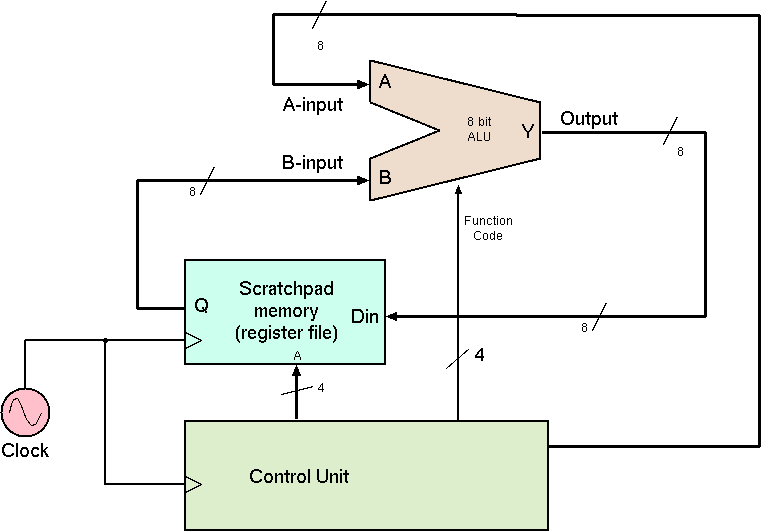
Combining the Execution and Control Units
Our Program Again
Computer Architecture (further reading):
The Future