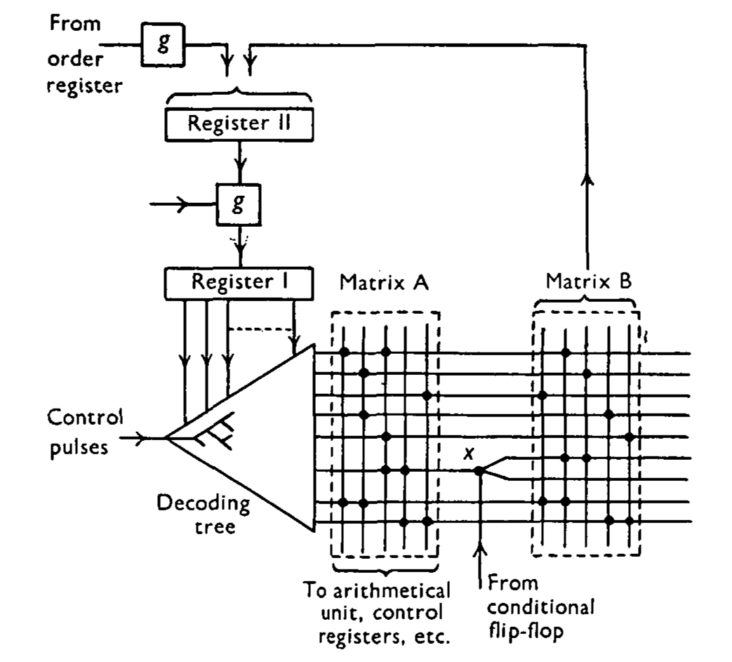
Figure 1 from Wilkes+Stringer 1952 'Micro-programming and the design of the control circuits in an electronic digital computer.
PAGE UNDER CONSTRUCTION 3Q2026
EDSAC-2 was arguably the world's first operational microcoded machine: certainly the first 'full-scale' machine. Actually, the documentation for EDSAC-1.5 is also in the DJW26 portfolio but I've not looked at it yet. Perhaps that was the first one?
EDSAC-2 ran each instruction by executing a sequence of micro-orders for each user instruction. The micro-program also implemented the exception and interupt mechanisms and the write-back generally necessary after a primary store read, since ferrite core has destructive read-out.
A 'horizontal' microcoding format was used, meaning it has unary micro-command encoding, with no subsequent binary-to-unary decoding from packed fields. A slight deviation in this approach applies to the next-instruction field too, which consists of two five-bit unary fields --- a two-digit number in base 5.
However, this is likely a description of EDSAC 1.5, since EDSAC-2's ROM was much larger. This is corrected here UPROG.
Wilkes had described techniques for micro-coding in Wilkes+Stringer53.
Figure 1 from Wilkes+Stringer 1952 'Micro-programming and the design of the control circuits in an electronic digital computer.
He went on to advocate the "Best Way" for designing microcode in MV Wilkes:: "THE BEST WAY TO DESIGN CALCULATING AN AUTOMATIC MACHINE" Volume 14 Part 2 pp 182-184 in THE CHARLES BABBAGE INSTITUTE REPRINT SERIES FOR THE History Of Computing. 1951. Reprinted in the Anals of the History of Computing .
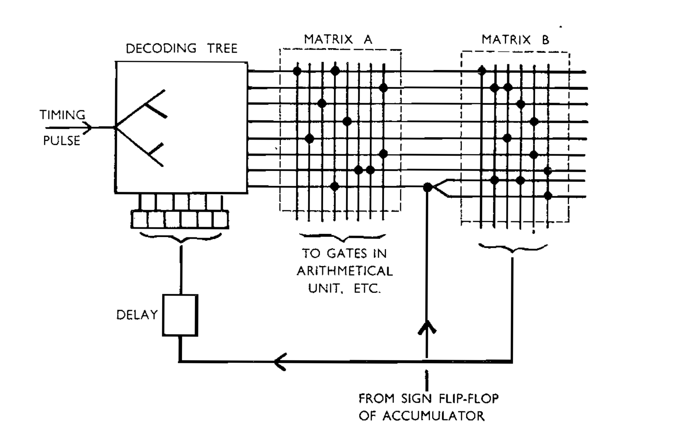
Similar image given from Wilkes' paper at the Babbage Institute.
But, the approach used in EDSAC-2 differed fairly radically from this 'Best Way' approach. Although he had pointed out that " quote needed " technology changes and a suitable mix of ferrite and diode ... He says he was asked to 'open up discussion', mentions pluggable microcode ROMs and finished with considering user-programmable microcode.
Nonetheless, the controller design used in EDSAC-2, as finally disclosed in Wilkes+Gill, is not really covered in his 'Best Way' review!
The microcode program counter needs a reset point (two are used I think owing to the clear-to-ones option - I will check), and it needs to advance from one micro-order to another, sometimes making a multi-way branch. As Wilkes suggested, optimsing the multi-way branch for order dispatch is a key consideration, as is selecting the balance between ferrite core and semiconductor diodes for the switching mechanics.
The method used in EDSAC-2 was reported in Wilkes+Renwick+Wheeler <.V. Wilkes, W. Renwick, and D.J. Wheeler, “The Design of the Control Unit of an Electronic Digital Computer,” Proc. IEE, Vol. 105B, 1958, pp. 121-128.
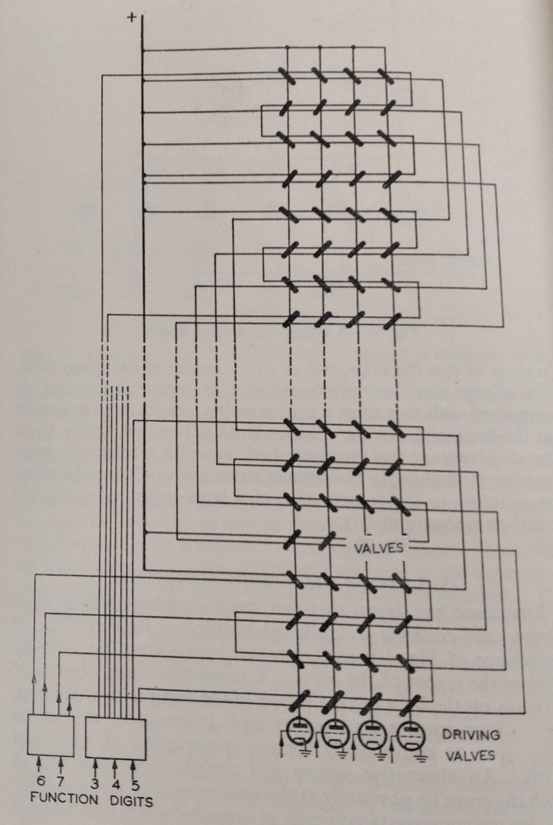
Figure 10 from Wilkes+Gill (an accurate rendition of the EDSAC-2 solution).
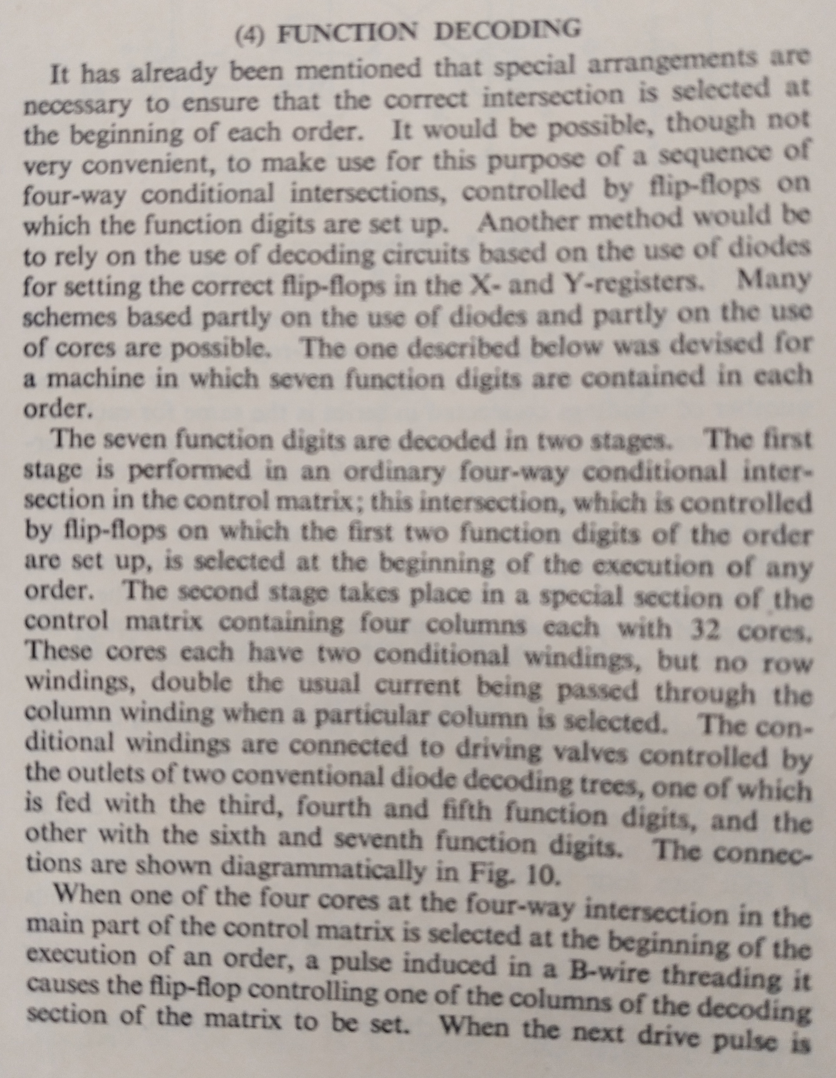
The key text from Wilkes+Gill that explains the instruction dispatch mechanics.
It has already been mentioned that special arrangements are necessary to ensure that the correct intersection is selected at the beginning of each order. It would be possible, though not very convenient, to make use for this purpose of a sequence of four-way conditional intersections, controlled by flip-flops on which the function digits are set up. Another method would be to rely on the use of decoding circuits based on the use of diodes for setting the correct flip-flops in the X- and Y-registers. Many schemes based partly on the use of diodes and partly on the use of cores are possible. The one described below was devised for a machine in which seven function digits are contained in each order.
The seven function digits are decoded in two stages. The first stage is performed in an ordinary four-way conditional intersection in the control matrix; this intersection, which is controlled by flip-flops on which the first two function digits of the order are set up, is selected at the beginning of the execution of any order. The second stage takes placed in a special section of the control matrix containing four columns each with 32 cores. These core each have two conditional windings, but no row windings, double the usual current being passed through the column winding when a particular column is selected. The conditional windings are connected to driving valves controlled by the outlets of two conventional diode decoding trees, one of which is fed with the third, fourth and fifth function digits, and the other with the sixth and seventh function digits. The connections are shown diagrammatically in Fig. 10.
When one of the four cores at the four-way intersection in the main part of the control matrix is selected at the beginning of the execution of an order, a pulse induced in the B-wire threading it causes the flip-flop controlling one of the columns of the decoding section of the matrix to be set. ...
Moreover, the four-quadrant binary decode is exploited in the micro-code to distinguish between 'modifier' and non-modifier orders.
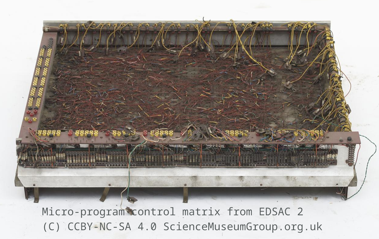
One instance (how many were there?) of the Microcode ROM
Unlike modern vertical microcode, the EDSAC-2 control matrix features no downstream binary-to-unary decoding. The 65 or so control lines operate entirely in parallel. A large number of these lines (or micro-commands) control transfers between architecural registers in the arithmetic, address and BIU units (CT1 through CT3). It is perfectly possibly to cause a bus fight by commanding more than one word is transferred to the same destination at once. But, these units are implemented with what we might call Resistor-Valve Logic (RVL) which is what one might call the valve equivalent of resistor-transistor logic. Unlike CMOS, such logic inherently functions as a wired-NOR, so activating multiple source lines simultaneously would not cause excessive current flow. However, it must be avoided for proper functionality. Avoiding concurrent drivers is one of the static side-conditions for the micro-code to be well-formed. Other conditions (mentioned later) relate to settling delays and shoot-through.
Each micro-order has a name and an address. The names broadly corresponded to the function. For instance, names starting with 'I' implement instruction fetch and those starting with 'J' implement jumps and branches. The address was two-dimensional, locating the micro-order in a 32-by-32 virtual grid. Each micro-order was held in the hardwired microcode ROM that was implemented with ferrite cores. The cores were placed in plastic holders, with up to 16 cores per holder and the holders being in something like an 8-by-8 grid. There could be up to four cores at a given address, owing to predicated operation (see below).
Each core implements a four-input AND gate whose output feeds some number of micro-command sense lines. The input terms and the output sense wires were all threaded through the core (number of turns on the sense wires was?). The microcode ROM data is represented by the physical routing of the sense wires thorough just the cores that should trigger it.
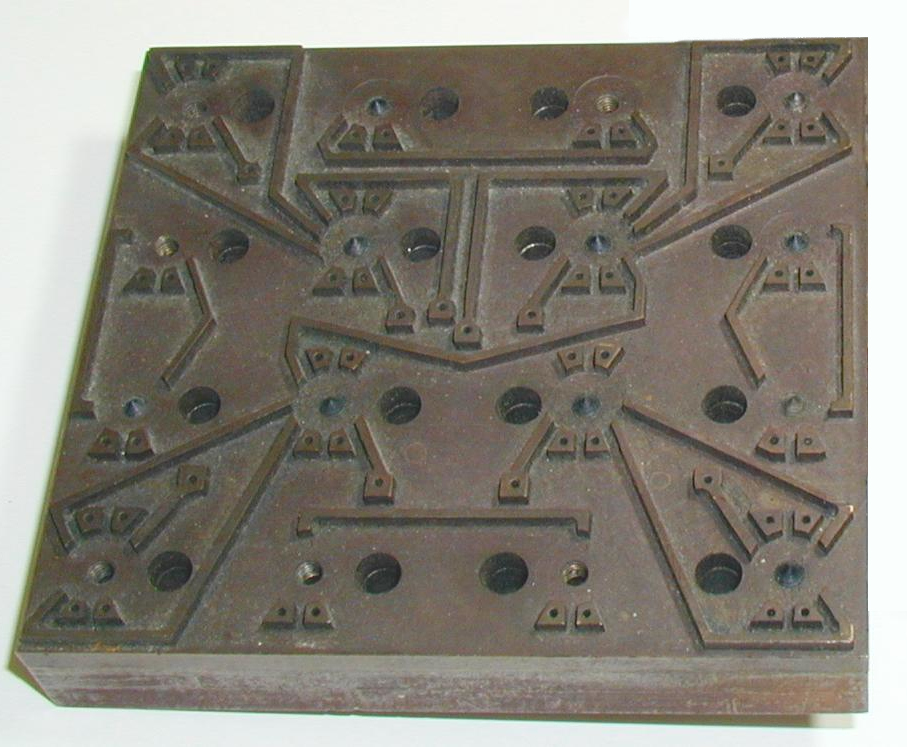
An EDSAC-2 microcode core holder or frame
A micro-order program counter of ten bits is implement across several instances of CT6.
The micro-order program counter addresses precisely one micro-order location. There are 1024 possible addresses and there is a one-to-one mapping between micro-order names and addresses. But more than one micro-order is often stored under a given name and address, with disjoint guarding predicates. The one whose predicate holds provides the next micro-order address. The successor is activated on the next clock pulse of the master clock. (Unlike EDSAC-1, EDSAC-2 was fully static and could be single-stepped one micro-order at a time, with the large 'engineer's display panel' of neon indicators showing the bits in all the registers and micro-architectural flip-flops.)
Two of the input wires threaded through a core correspond to the row and column of the core's address. Up to two further 'conditional bias' wires provide conditional operation. Conditional operation is needed for user-level IF-THEN logic required for conditional branch orders. But it is also needed for microcode level loops, such as long multiplication and floating-point normalisation steps. Finally, conditional operation also supports something akin to subroutine calling at the microcode level.
These microcoded 'subroutines' are not implemented with a saved return address. They are just a means of invoked a shared common sequence of operations from more than one call site. This is achieved with the provision of so-called 'Y' flip-flops, that the microcode can freely set or clear before jumping to a shared sequence. The sequence is terminated with jumps conditional on the 'Y' flops so that the next step accords with the 'callers' intentions.
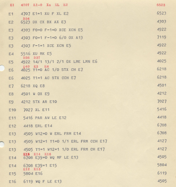
EDSAC 2 Microcode Example - Fixed-point Multiply. As scanned.
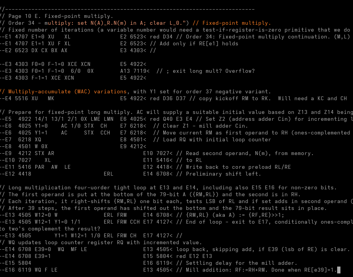
EDSAC 2 Microcode Example - Fixed-point Multiply. As OCR'd, corrected and hard-annotated.
| Mnemonic | Function | EDSAC | Verilog |
|---|---|---|---|
| C | Arithmetic mill carry bit | ||
| CC | Address unit carry bit | ||
| E1 | Master section for extended precision accumulator: a mantissa bit | RE[e1] | RE[v38] |
| E31 | Master section for extended precision accumulator: LSB of mantissa | RE[e31] | RE[v8] |
| E39 | Master section for extended precision accumulator: LSB and LSB of exponent | RE[e39] | RE[v0] |
| F-1 | Master section of the accumulator: Bit -1 is the carry bit. | RF[e-1] | RF[v40] |
| F0 | Master section of the accumulator: MSB. | RF[e0] | RF[v39] |
| F1 | Master section of the accumulator: bit below MSB. | RF[e1] | RF[v38] |
| F32 | Master section of the accumulator: MSB of exponent field. | RF[e32] | RF[v7] |
| G10 | Synchronised version of input ready/synch. Updated by BG. | G10 | G10 |
| G9 | Synchronised version of output ready/synch. Updated by BG. | G9 | G9 |
| M-1 | Accumulator register: Bit -1 is the overflow bit. | RM[e-1] | RM[v40] |
| M32 | Accumulator register: MSB of the exponent field. | RM[e32] | RM[v7] |
| P19 | Program counter: LSB, used for lane steering, odd/even halfword. | RP[e19] | RP[v0] |
| W9 | MSB of the address adder result register, RW. | RW[e9] | RW[v11] |
| W12 | Bit 8 of RW, for microcoded normalisation and rotate loops etc.. | RW[e12] | RW[v8] |
| X0 | MSB of ordercode (upper modifier bit) | n/a | x20[v19] |
| X1 | Second bit of ordercode (lower modifier bit) | n/a | x20[v18] |
| X2 | MSB of order number | n/a | x20[v17] |
| X3 | Second bit of order number | n/a | x20[v16] |
| X32 | Floating point mystery flag? PLEASE EXPLAIN ME ! | RX[e32] | |
| Y1..Y4 | Microcode control flow routing (rail track points). Y2=alpha. | Y{1..4} |
The table below lists all fo the micro-command control wires are used in the microcode. As mentioned above, these are 'horizontal' control wires that are directly driven sensed from the threading of a sense wire through a ferrite core in the control matrix and they are not subsequently unpacked in any way, such as with binary-to-unary decoders.
There are 65 of these, if I have accounted correctly.
The maximum number of core sense wire threaded on a core is ... about 5 of these plus a further two to select the successor micro-instruction.
DJG status: The wiring and semantics for the marjority of them is now understood.
| Name | Semantics | Description |
|---|---|---|
| 0B | =0/BMFF | JJ60: RBM Reset blockmark (CT7 schema) |
| 0X | =0/RX | JJ27: clear RX |
| AC | See text | JJ12: See the light font sheet that did not OCR please. |
| AI | INPUT<<20/RI | JJ58: Activate input. Transfer date from the selected peripheral to RI input register. |
| AO | RD/OUTOUT40 | JJ59: Activate output. Instruct peripheral to process RD contents. |
| AR | Mem[RP]/MDRX | JJ28: Activate Read. (Destructive) read of addressed primary store word. |
| AW | RX/Mem[RP] | JJ29: Activate write. Write to primary store. |
| AX | Z5?RF[e0..8]:RW[e3..10]/RX[e0..8] | JJ21: Update RX[e0..8] (high word function part). |
| BX | Z5?RF[e9..19]:RW/RX[e9..19] | JJ22: Update RX[e9..19] (high word address part). |
| CX | Z5?RF[e20..28]:RW[e3..10]/RX[e20..28] | JJ23: Update RX[e20..28] (low word function part). |
| DX | Z5?RF[e29..39]:RW/RX[e29..39] | JJ24: Update RX[e29..39] (low word address part). |
| BGG | Z4/G2 | W54: Z4G2 or is it P19/G2 most/least |
| CCH | ~RC[e0..39]/RH[e0..39];=0/RH[e-1] | JJ2: Transfer one's complement of RC to RH. |
| CH | RC/RH | JJ1: Transfer RC to RH. |
| ELL | RE<<1+Z1/RL | JJ13: Transfer RE left-shifted one with Z1 in lsb to RL. |
| EOLO | RE[e-1..0]/RL[e-1..0] | Xfer overflow+sign from RE to RL |
| ERL | {RF[e39],RE[e1..38]}/RL | JJ14: Transfer RE right-shifted one to RL. 39 bits only, with msb sourced from RF[e39] |
| Fe | MADDER/{dustbin32,RF[e32..39]} | JJ19: Exponent part of data mill addition - alternate spelling. |
| FE | MADDER/{dustbin32,RF[e32..39]} | JJ19: Exponent part of data mill addition |
| FLM | {RF[e0..39],RE[e1]}/RM | JJ6: Transfer RF left-shifted one bit to RM |
| FN | MADDER/{RF[e-1..31],dustbin8} | JJ16: Data mill addition. Bits 0 to 31 |
| FRM | {RF[e-1],RF[e-1..38]}/RM | JJ7: Transfer RF right-shifted one bit to RM. |
| F | MADDER/RF | JJ19+JJ15 - full mill addition, updating all of RF. |
| IGG | =1/G2 | JJ47 (aka OGG?) sets the lane steering flop G2 |
| IG | =1/G1 | JJ51: (aka Z4G1?) set Free/Wired flop G1 |
| INX | RI/RX | JJ56: Load from input register RI. |
| IX | RI/RX | JJ56: Input READ alternative spelling. |
| KC | RK/RC | JJ3: Transfer RK to RC. |
| LE | RL/RE | JJ15: Transfer RL accumulator (lower half) to RE (master section). |
| LME | RL[e32..39]/RM[e32..39] | JJ9: Transfer RL to exponent[e32..9] of RM |
| LMN | RL[e-1..31]/RM[e-1..31] | JJ8: Transfer RL to carry and mantissa of RM |
| MF | RM/RF | JJ18: Transfer short accumulator M to RF (master section). |
| MK | RM/RK | JJ10: Transfer FRM to RK. |
| OG | =0/G1 | JJ50: clear Free/Wired flop G1. (labelled spare on CT7 schema.) |
| P19G2 | P19/G2 | JJ53 W53: P19GT. |
| PAR | ??? | W55: Parity result to G14. |
| PGG | P19/G2 | JJ52 W52? Lsb of RP to flop G2 (lane steering). |
| PR | RP/RR | JJ45 or W45: PC commit. |
| P | CADDER/RP | JJ26: Control adder (RQ+RU+Z2) result to RP. |
| RQ | RR/RQ | JJ37: Transfer RR to RQ. |
| R | CADDER/RR | JJ44/W44 Controll adder (RQ+RU+Z2) to RR (aka PC). |
| SGG | INSYNCH/G10;OUTSYNCH/G9 | Fetch/poll I/O ready status. |
| STX | RX|MDRX/RX | JJ30: Complete read, AC or bitwise OR. |
| SW | RS/RW | JJ33: Transfer RS to RW. |
| TW | RT/RW | JJ32: Transfer RT to RW. |
| WCU | ~RW/RU | JJ42: Transfer one's complement of RW to RU |
| WGM | RW[e19]/G6;RW[e18]/G7;RW[e17]/G8;RW[e14]/G11;RW[e12]/G12;RW[e15]/G3 | W49: WGM Register 'w' to G6,G7,G8, G11, G12, G13 . Mag tape control [Sel; Sel; Sel; Read/Write; Forward/Back;Record BM Off/On] |
| WGT | RW[e19]|!RW[e18]&G3/G3;RW[e15]|!RW[e14]&G5/G5;RW[e16]|!RW[e17]&G4/G4; | W48: WGT Register 'w' to G3, G4, and G5. Paper tape |
| WQ | RW/RQ | JJ36: Transfer RW to RQ. |
| WS | RW/RS | JJ39: Transfer RW to RS. |
| W | CADDER/RW | JJ31: RW := RQ+RU+Z2. |
| WT | RW/RT | JJ34: Transfer RW to RT. |
| WU | RW/RU | JJ41: Transfer RW to RU. |
| XCE | x40[v7..0]/RC[e32..39] | JJ5: Transfer RX to exponent8 of RC. |
| XCN | {x40[v39],x40[v39..8]}/RC[e-1..31] | JJ4: Transfer RX to mantissa32 of RC with sign extension. |
| XD | RX/RD | J57: Store data in output register, ready for punch (or other peripheral). |
| XL | {x40[v39],x40}/RL | JJ11: Transfer RX to RL |
| XQ | x11/RQ | JJ38: Transfer x11 to RQ. |
| XS | x11/RS | JJ40: XS or XDM in places. |
| XT | x11/RT | JJ35: Transfer x11 to RT. |
| XU | x11/RU | JJ43: Transfer x11 to RU. |
| Z3G1 | Z3/G1 | JJ52 W52??: Select fixed/free memory page (data or code?). |
| Z4G1 | Z4/G1 | Select fixed/free memory page (code or data?) |
| ZGG | =0/G2 | Clear half-word steering flop. Allows full-word load from RX to mill. |
| ZL | unknown |
AC - activate constant - loads a pre-selected hardwired value into the core-store data register (not RX directly). The value is commonly (always) then transferred into RX using STX. RX is normally (always?) cleared first, so the fact that STX used a bitwise-OR into RX is (generally?) immaterial. NB: STX having that disjunction semantic is exploited in the disjunction user-level instruction, order XX.
Z13?=89<<20:=512<<20/MDRX;=0/Z12;=0/Z13;=0/Z14;=0/Z15
Activate constant table of values and Zflop reset ...
A table of constant values for AC does not appear to be present in DJW26. It was relatively easy to work out the Z-flop values present at each use site, but only some of the associated constants have been determined so far.
TABLE OF AC CONSTANTS ...
Unlike modern vertical microcode, the EDSAC-2 control matrix features no downstream binary-to-unary decoding. The 100+ control lines operate entirely in parallel. Because the underlying Resistor-Valve Logic (RVL) inherently functions as a wired-OR, activating multiple source lines simultaneously does not result in a structural decoder error, but merely causes a benign bus overlap. To reflect this unencoded, direct-drive architecture, the individual control units of the micro-instruction word are referred to here as gate wires. A large number of these are 'transfer pulses' which cause the transfer of a word from one register to another, with no distinction between architectural and micro-architectural registers.
Basic validation conditions:
Micro-order names and addresses validation There should be no repeated names or addresses, except where predicates differentiate. Correct (systematic) correspondence between micro-order names and addresses.
While the underlying Resistor-Valve Logic (RVL) safely resolves concurrent bus drives via a wired-OR, the microcode was hand-crafted to avoid bus contention. The validator enforces a mutual exclusion (mutex) constraint on all gate wires sharing a common destination bus, confirming that no microinstruction accidentally commands multiple sources to drive the bus at once.
No path should exist generated by simultaneously enabling the leader (master) and follower (slave) transparent latches that we would now recognise as the essence of an edge-triggered transfer (or dual-phase non-overlapping clock). In modern synchronous design, this would violate the non-overlapping clock phase constraint and cause a hold-time failure.
A control-graph trace ...
Apart from the halt and stop-report states, every micro-order should have a successor, regardless of the predicate (sense wire) combinations.
The number of micro-commands threaded by a core should be bounded for physical realisation (getting the wires through) and noise margins.
If the same sense wire threads more than a certain number of cores in a given row or column, the systemmatically accumulated EMF as that row or column wire is driven could give a false reading. Hence, in XXX it says the maximum number of such threadings is limited to 4. The layout was optimised using EDSAC-1 and is cited as one of the eariliest examples of computer-aided design (CAD) or electronic design automation (EDA).
The result from an addition or other slower operation should not be used in the next micro-order.
A read from primary storage should be written back afterwards unless explicitly due to be modified.
Two simulators have been written. A low-level one steps through each micro-order in turn. The higher-level one is based on a basic-block conglomoration of micro-code addresses with the large-step operation semantics symbolically extracted from each block. ... under construction ... August 2026.
... under construction ... 2H2026
(C) CC4BY 2026 DJ Greaves, University of Cambridge.