DJW26 EDSAC-2 Portfolio - A First Study - Microcode and Architecture Analysis
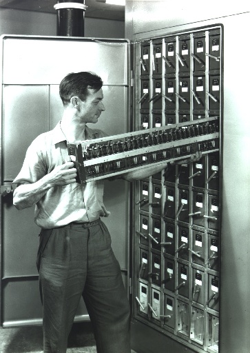
EDSAC-2: Sid Barton replaces an EDSAC-2 chassis in the machine.
One paragraph summary:
EDSAC-2 replaced EDSAC-1 in 1958.
It was the first full-scale micro-programmed machine and also the first bit-sliced machine.
As can be seen from the photo, the individual chassis were easily replaceable (much more so than those of EDSAC 1) so it was easier to maintain.
It was also much easier to use.
It used fast paper tape for I/O and later became one of the first machines to use magnetic tapes.
Other output devices included a line printer, a curve plotter, a photographic imager and two high-speed paper tape punches.
It had many hundreds of users, and two Nobel prizes arose from work done with it.
EDSAC-2 was turned off in 1965 and replaced by TITAN.
Output from a microcode-based EDSAC-2 simulator running hello_world.eds in 2026.
Introduction
EDSAC-2 was designed and built in the University of Cambridge Computer Laboratory. It provided the main computing service for
the University between 1958 and 1965. It implemented floating-point (32-bit mantissa with 8-bit exponent) and followed the von Neumann
stored-program design pattern. Primary storage available to the user initially consisted of 1024 words of 40 bits, addressable in half-word
locations. A second fixed-store contained a permanent library of scientific, I/O and debugging routines, with a special instruction implemented
to invoke these routines (the 59 Order).
The principal improvements over the world-leading EDSAC-1 computer, that was its predecessor in the department, were:
It was microcoded, enabling floating-point arithmetic and other advanced facilities to be implemented in the instruction set.
It was fast, owing to being bit-parallel, performing a complete 41-bit addition in one microcode step.
It was almost completely static, enabling single-stepping at an instruction or micro-op granularity, with all register bits displayed on a large panel of neons.
The hardware used a bit-slice approach, with pluggable modules that could be tested outside the machine and quickly replaced for low down time.
Following on from the famous "Initial Orders" of EDSAC-1, the reserved store contained a built-in assembler/loader (essentially an operating system) that made it as easy to use.
The basic architecture can be summarised as A10D40, meaning it addressed 1024 40-bit words. But it also supported half-word
addressing of the main store (A11D20 style). But more memory than address space was
available in reality, since there were two primary stores, known
often as 'free' and the 'reserved', selected between with an additional address bit held in a control flip-flop.
In mid life, (possibly November 1962) the architecture was augmented with an additional index register, RB, that was 14 bits in width, instead of the 11 bits used in all other address-unit registers.
This was one means to
address the so-called 'main' store of 16386 words that was added. Since the term 'main store' has a very specific meaning in the EDSAC-2 context, it
is helpful to not use that term for the primary store. (Primary storage is what can be addressed directly in the instruction set.) The ISA was
accordingly extended with several orders (instructions) to support the
main store, but the DJW26 portfolio does not appear to contain any main store circuits
or information.
A full specification of the programmer's view, however, is given in "PROGRAMMING FOR EDSAC 2 WITH MAIN STORE", 1962, by D. Barron (linked below).
Regarding the above 'classic' photo of S Barton replacing an EDSAC-2 chassis, Frank King commented in 2026:
"I remember David Barron coming to Cambridge to speak at a David Wheeler memorial event [in 2005]. He showed this picture and pointed out that this absolutely wasn't how a chassis was changed. I think he said that the machine was almost never switched off and changing a chassis would be done with everything running. Even standing nearby was like standing next to a furnace. To change a chassis required wearing massive gloves and other protective gear."
An example EDSAC-2 program with annotations from Frank King ...
DJW26 Portfolio Binders of Schematics and Microcode
DJW26: The six portfolio binders received.
In 2026, a set of six portfolio springback binders of EDSAC-2 schematics together with a microcode listing and other documents was returned to the Computer Laboratory. This came from the house of DJ Wheeler, so it is currently called the DJW26-portfolio. The binders will be handed over to the University Library soon. Meanwhile, these materials are being studied. Some preliminary findings are being put on this page. Also, interviews with extant users have been recorded and can be released soon and the classmark added here.
A complete reverse-engineering and proof of correctness of the EDSAC-2 microcode, based on the DJW26 portfolio, is being assembled on these pages and will be written up as a white paper.
Another set of valuable resources was supplied by Geoff Daniell and is here known as the GJD archive. (Note: DJW, DJG and GJD have very similar initials!)
DJW26 Inventory
A preliminary listing of the portfolio content. I will increase the level of detail here...
Binder Volume 1 - Chassis
Register of Inter-connections of EDSAC II diagram
EDSAC 2 Engineering Manual - Table of contents, significance of the Digits in an Order, The Functions of the Edsac2 Chassis, Chassis Power CONNECTIONS. PDF
Chassis 16 - "Y" and "Z" flip-flops [two pages] PDF
Chassis 17 - Start=stop and Function Decoder Row Drive Unit PDF
EDSAC 2 - Vol. 2 - Miscellany
Peripheral Items
Miocroprogram (MK 1)
Wired Store Programs (ie Fixed-store subroutine listings).
EDSAC-1-1/2
EDSAC 2 - Vol. 3 - Line Printer
This folder is very interesting - no valves, but transistors and a ferrite core shift register! [FIFO queue? ]
Not yet digitised by DJG.
EDSAC 2 - Vol. 4 - High Speed Punch
Not yet digitised by DJG.
Creed High Speed Punch with check back. Type 3000. Circuit Manual - February 17th 1962
Again, this is transistorised (OC44 etc) but with some ferrite logic.
General Operation
Data
Circuit Conventions
Basic Circuits
Circuits
Error Detection System Notes
Binder 5 - Also labelled High Speed Punch - ("DJ Unwin, Magrath Avenue, Cambridge" is stamped inside front cover).
Not yet digitised by DJG.
Enclosed is a document entitled - "The Line Printer Buffer Store" that starts 'In order to make the best used of the "Hollerith" Parallel Printer on EDSAC 2 a buffer has been built. It consists of 80 x 12 ferrite core store and a number of flip-flops ...'
Otherwise, this might be a copy of Vol.4 - we need to play spot the difference.
Binder 6 - Line Printer
Not yet digitised by DJG.
This springback binder contains a single sheet - a schematic for some ferrite logic.
As well as the six springback binders, there is an unbound pile of dyeline schematic prints. From the page titles, these
appear, for now, to be schematics for the line printer and were probably in Binder 6 at some earlier time...
Current Status of this Analysis (September 2026)
The schematics from binders 1 and 2 have mostly been digitised. The microcode had been OCR'd and largely validated for self-consistency.
Operational semantics have been written for
each VLIW operation (micro-command) invoked by the microcode. This has formed the basis for a microcode-based simulator/emulator
that has run the 14580 instructions of the hello_world.eds program supplied in the GJD archive.
That program writes Hello World in dot matrix form on the display CRT, one of the output devices connected to EDSAC-2.
As well as the application, the fixed-store contents had also to be assembled into machine code and loaded
into the emulator, alongside a model of the paper-tape reader and the microcode itself. The CRT output was collected in a file
and viewed with Gnuplot. A few mistakes in the microcode have been fixed and 3 extended ISA instructions had to be
implemented in fresh microcode. The average CPI is about 13. Micro-order coverage is ... A proper report will follow ...
... Coverage : 236 distinct micro-order addresses used out of 847 (before DJG ISA extensions)
EDSAC-2 Ordercode Summary
Unlike EDSAC, EDSAC-2 did not use mnemonics for machine orders (instructions). They are simply numbered in decimal, but
with some structure to the pattern as expressed in base 10, so that they might be easier to remember.
Here is a handy sheet giving a summary of the order codes and fixed-store routines from 1960.
EDSAC-2
EDSAC-2 Memorandum No 19, Summary of Ordercode, etc.. Click for higher resolution.
But one aspect of the underlying binary coding is manifested in special 'modifier' semantics for instructions between 64 and 95.
The full details that a programmer should need are given in the following booklet.
Three editions were issued as the architecture was revised. This is the first edition. We don't currently
have a second edition. The third edition was scanned as part of the GJD archive and (will be) attached below.
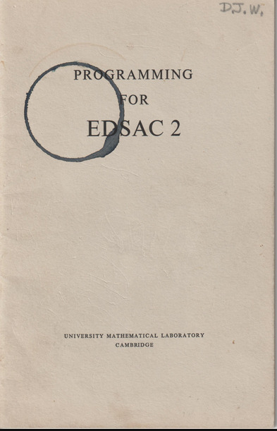
Booklet: Wilkes 1958: Programming For EDSAC 2 PDF
DJW26 A First Study - Overview
EDSAC-2 Microprogram core matrix (32x32) with drive valves directly adjacent and then control and sense chassis around the edges.
A Note on EDSAC-2 Terms and Notation.
Naming:
EDSAC-2 uses single-letter acronyms in most places, such as 'M' for the accumulator.
This is painful for the modern user, or when coding the semantics formally, or just when searching textually for
a given item. With only 26 letters in the arabic alphabet, letters are commonly reused for different things,
although a partially complete disambiguation sheet is provided in the DJW26 documentation. In this analysis, I have avoided
single-letter names for those reasons. I have lightly renamed. For instance, I have put the letter 'R' in front of all the register names.
Bit numbering: The 41-bit registers are indexed -1 through to 39. The nominal most-significant bit is bit 0, with bit -1 being
used for carry and overflow detection (except in memory, where it is a parity bit). Bit 39 is the least-significant bit when holding
a fixed point fraction. The 11-bit registers are indexed 9 through to 19.
For example, using the notation introduced in the next paragraph, RW[e9..19] denotes the whole of register RW. These bit
names are used since they align with the same bit numbers in RX when data is transferred to and from RX in the BIU for memory (or conceivably I/O) into the control unit registers. Actually, there is lane steering (controlled by the G2 flip-flop), so when loading from an odd address, it is bits RX[e29..39] aka RX[v10..0] that are moved to or from RW[e9..19].
Bit inserts and bit extracts: Since part of this analysis emits the EDSAC-2 design as Verilog, and since modern computing generally
numbers bits from the right with positive integers, it is necessary to distinguish between bit-fields expressed in EDSAC form from those
expressed in standard RTL. Here we distinguish EDSAC with conventional bit numbering by inserting either the letter 'e' or the letter 'v' (for Verilog)
right after the open square bracket.
For example, the program counter (or sequence control register) in EDSAC-2 is RR. It has 11 bits.
Both RR[e9..19] and RR[v10..0] denote the whole of register RR, as does not bit-indexing it at all.
Note: the EDSAC bit numbering makes sense for the arithmetic mill registers, as the numbering is the power-of-two weighting (if negated) for fixed-point
fractions (as explained in Programming For EDSAC-2).
Registers in Memory: EDSAC and EDSAC-2 refer to an instruction as an 'order' and the opcode is an 'ordercode'. This causes little trouble
to the modern reader. On the other hand, the terms 'registers in memory' and 'memory registers' are used in the EDSAC documentation. This is too jarring
for the modern reader, I fear, so I have modernised and use the term 'location' to denote a place in memory. Note that the EDSAC-2 memory bus has a word width of 40 bits
(plus parity). That is the same length as the accumulator register RM (after ignoring the carry/overflow bit). But instructions are 20-bits long, with two being fetched over the memory bus at once.
I shall call the 20-bit quantity a half-word, with the bus transferring a whole word at once. The memory itself is half-word addressed. Hence the 11-bit program
counter RP, or any other modifier register etc., points to memory on a half-word granularity. EDSAC-2 is big endian, meaning the high order 20 bits
of a word are addressed when the lsb of RP, ie RP[e19] or RP[v0], is zero.
Regarding the memory parity there is currently a small mystery.
Parity is implemented in Chassis CT3 according to the notes relating to the inter-bit wiring that are bundled with the schematics. But none of the required XOR gates seems to be present and the
parity connection pins on the backplane (if I may call it that) connector may be confused with the lane steering 'output gate' logic. Investigation ongoing...
Control Panels and System Layout
Operator's Control Panel
The operators panel houses all of the main, day-to-day controls, needed to
operate the machine. At the top right are the power status indicators and on/off buttons in three
groups, labelled MAIN AC, HT and AUX AC.
At the top left is the 'manual register'. This consists of 40 post office keys in four
columns with rows numbered 0 to 9. A 40-bit binary number can be manually entered.
Its value can be read by op120. op120 can also read a timer and
stop the machine based on a mask applied to certain other front panel
keys - the optional stop keys.
A vertical row of indicators numbered 1 to 1024 (11 off) shows in binary the
address where the machine has stopped from order 101 or 102. The additional indicators
for 'free' and 'reserved' show one further effective bit of address. Code cannot be
executed from the later-added 'main' store, so a stop in main store did not become possible.
Buttons for 'Run', 'Set start' and 'Clear to ones' force control to the start of the microcode, clear the memory to all ones, clear the CRT display and commence execution.
Other switches enable or swap over the paper tape readers and turn
on or off the three punches and the line printer.
A large yellow indicator marked PUNCH ERROR shows that the readback after punching a row of paper tape failed to compare correctly.
A volume control adjusted the speaker volume. It was common to 'listen' to the sound of early computers by
connecting an amplifier to one or two bits of appropriate registers.
GJD writes "The loudspeaker on EDSAC2 was connected to the 32 bit of the address
part of the current instruction". The following sound file was recorded on the original machine, perhaps using Richard Jennings music compiler
.
There are various other indicators and controls. A full description of
how they worked is not yet to hand, but the GJD simulator implements many of them.
Engineer's Control Panel
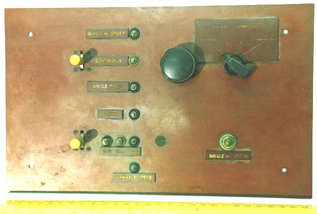
The Engineer's control panel enabled the clock frequency to be adjusted. Two fixed rates were supported, with a third setting
allowing a variable capacitor (rotary knob) to set the speed. Single step was also supported, at a micro-order or user-level order
granularity. The engineer stepped the program by pressing a button. They would watch the status in binary of
all of the registers in the machine (not memory locations of course).
Engineer's Display Panel
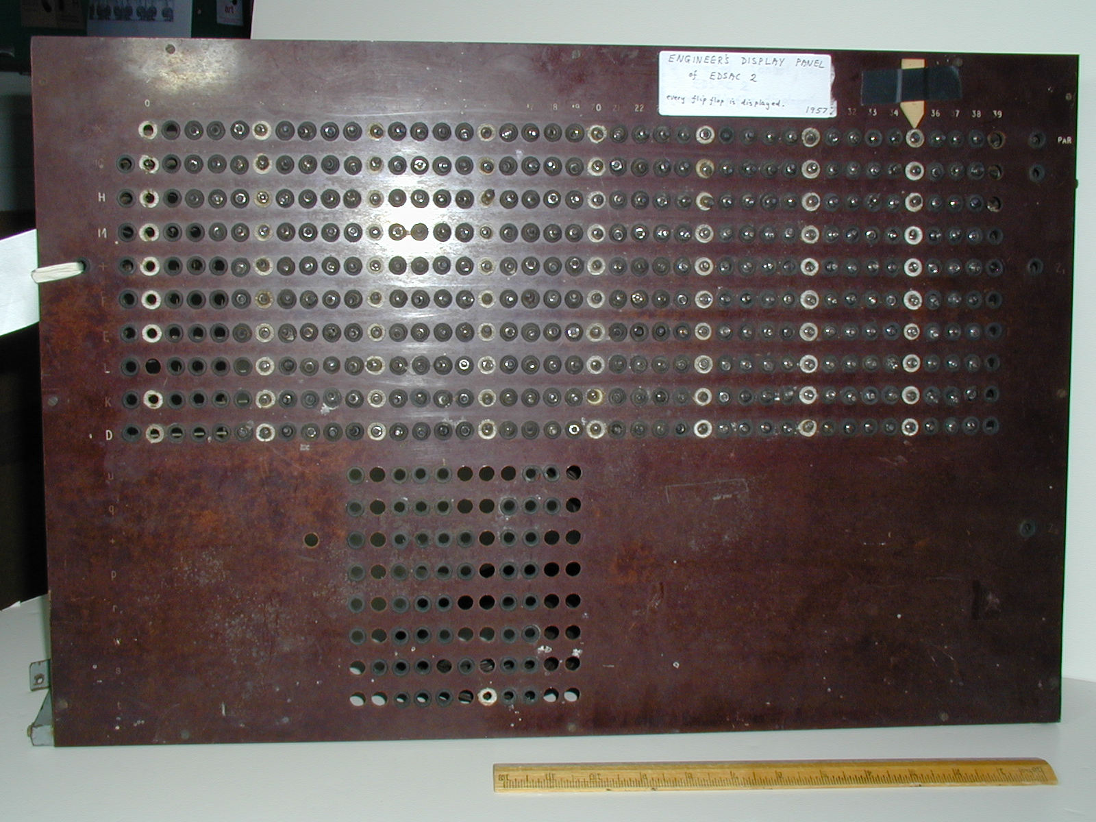
Every flip-flop on every chassis was rendered on this large panel of neons. The top section shows the 41-bit registers
of the arithmetic mill and RX, which is 40 bits.
An extra indicator on the right shows the parity bit for RX, RC and +? (power?).
Reading from the top, the registers are RX, RC, RH, RM (the accumulator), +?, RF?, RE, RL, RK and RD.
The lower half shows the status of the 11-bit addressing/modifier registers, in the order RU, RQ, +?, RP, RR, RW, RS and RT.
DJG: surely, when single-stepping by micro-order we'd ideally want to see the micro-order program counter bits, which nominally has 10 bits. But since this was implemented as the product of two 32-bit one-hot encodings, this must have been displayed elsewhere, if at all.
EDSAC-2 Architectural Block Diagram
EDSAC-2 CPU overall architecture (excluding peripherals)
The principle components of EDSAC 2, like any von Neumann computer, are the execution unit, the control unit, the primary storage and
the peripherals.
In EDSAC 2, the execution unit has two distinct parts: the arithmetic mill (a djg name), implemented with 41 instances of chassis CT1
and the address unit that is implemented with 11 instances of CT2. The central bus interface unit (BIU) connects
everything together. The BIU uses 20 instances of CT3, which are a two-bit slice. Multiplexors inside CT3 implement the lane
steering translations needed to store 20-bit half-words in 40-bit full words.
The EDSAC 2 control unit is famously microcoded. The microcode is implemented with a hardwired matrix of ferrite beads that
act as a ROM.
The primary memory for EDSAC 2 is 40 planes of ferrite cores, supporting storage of 40-bit words.
The data wires connect to the CT3 instances and address bits are hardwired to RP. An additional, high-order address
bit comes from the reserved/free control flip-flop. This is slaved from a similar flip-flop that is logically an extension
of the PC (normally held in RR), but sometimes overridden when a reserved-store instruction needs to access the free store (or vice versa).
The I/O devices were connected to 40-bit input and output busses. These connect to the CT3 instances as well. Additionally, control
and status wires connect to the CT11 (and CT10?). Interrupt wires are ... text not yet ready ...
EDSAC-2 CPU Micro-architecture
EDSAC-2 CPU Micro-architecture and Primary Storage Connections
Concentrating now on what we'd now call the CPU, the EDSAC-2 central processor unit divides into two main parts plus the memory and I/O BIU third part.
The arithmetic mill is shown at the top. This is implemented using 41-bit registers and an adder.
The user programming model registers are M, L and K, are here marked RM, RL and RK.
The precision is nominally 40 bits, with the extra but, designed -1, serving as a carry or overflow bit. The extra bit
is not used at all for various of the registers, so conceivably the valves were not installed on the -1 chassis, but this
would require extra-care when hot swapping.
The extended precision available when RM and RL are paired is an extra 39 bits. This is because the zeroth bit of RL is bypassed
in the carry and rotate backplane wiring. DJG: I can see no reason for this decision, even though the zeroth bit is nominally
the sign bit, it has no specialised behaviour hardwired, so a full further 40 bits of precision should have been readily available?
Each register is implemented as a broadside transparent
latch, so, to achieve a master-slave edge-triggered effect, such as when left-shifting the accumulator,
the current contents need to be explicitly transferred into a master section, such as RF for RM using one
microcoded step and then transferred back again, modified accordingly. Hence, the system operates a bit like
the 8008 microprocessor, being based on two-phase, non-overlapping clock signals.
The address/modifier unit is shown lower left. It has a second adder, the address adder. The registers that
form part of the user's programming model are RB, RS, RT and RR. RR is the program counter.
Again, these are all transparent latches, so the same shoot-through considerations apply regarding permissable simultaneous transfers, both within the address/modifier unit and, more generally, between all CPU component registers.
In later
versions of EDSAC-2, a further modifier register, RB was added, presumably to this unit, and supported with new instructions and as implemented in the GJD simulator. This is not documented in DJW26.
The bus interface unit (BIU), which also serves for I/O is shown centre right. This contains the RX register that is the source
and destination for all data entering or leaving the CPU. It also contains a further 40-bit register, RD, where output data to peripherals is first stored.
Note that memory is always physically accessed at the full-word addressed by the top ten bits of RP, i.e. RP[v10..1]. Hence directly addressable memory in EDSAC-2 is 1024x40 or 1024 words, each of 40 bits. Half-word extract/insert logic in CT3 supports half-word operations at the ISA level.
EDSAC-2 Memory
Contemporary parlance divides computer memory into registers, main (aka primary) store and secondary storage (e.g. tapes, disks, SSDs).
EDSAC-2 has the the same three forms in its memory hierarchy. [DJG will add a note about caches here, known as the slave store.]
Unfortunately, 'main memory' has a special meaning in EDSAC-2 terms. It refers specifically to 16k words of primary store that
were added to the machine at a date seemingly after anything in the DJW26 portfolio. Hence we have a potential source of confusion of terms here!
As already mentioned, EDSAC-2 has a 1024x40 primary storage address space. This is used for both code and data since it is essentially
a von Neumann machine. But, even without the 'main store' extension, this address space is replicated two-fold, being partitioned into
the reserved and the free 'pages' or 'segments'. The 1960's documentation does not use such a terms: it just speaks of two stores.
The reserved store is very commonly also known as the 'fixed' or 'wired' store. But strictly a distinction should be made.
The reserved store address space is partitioned. The first quarter (0x000-0x1FF) is read/write RAM used as scratchpad
and buffer space for the library routines. The library routines were stored in the remainder (0x200-0x7FF) that was a fixed ROM.
containing permanently-installed subroutines. These routines are invoked with a dedicated instruction (order 59) whose microcode saves the user program counter (that addresses the free store) and commences operation in reserved address space. The ROM data is encoded
using a fixed, manual threading of priming wires into the fixed-store cores.
Therefore, the machine is not strictly von Neumann, and a further complexity
when executing out of fixed store is that certain instructions can access data in the free store! The
precise semantics of these is documented as 'guessed' in the GJD simulator. But an explanatory note in DJW26 and inspecting the microcode from DJW26 are shining a light ... TBC.
Since ferrite core store has destructive read out, operands and instructions read must be written back again to implement the conventional
paradigm of non-destructive read. In EDSAC-2, the write-back process is manifest as an explicit step in the microcode. But, in
cases like an exchange instruction or a store of just one half-word to a 40-bit word, the data written back is accordingly not
the same as the data read. Hence, no write lanes, as we'd call them today, are needed for primary store writes.
Write-back was not needed for the fixed-store, but was done anyway since much of the microcode is ignorant of which store it is currently using. Indeed, as explained below, the fixed-store content was written into it by the priming wires in advance of every read from it.
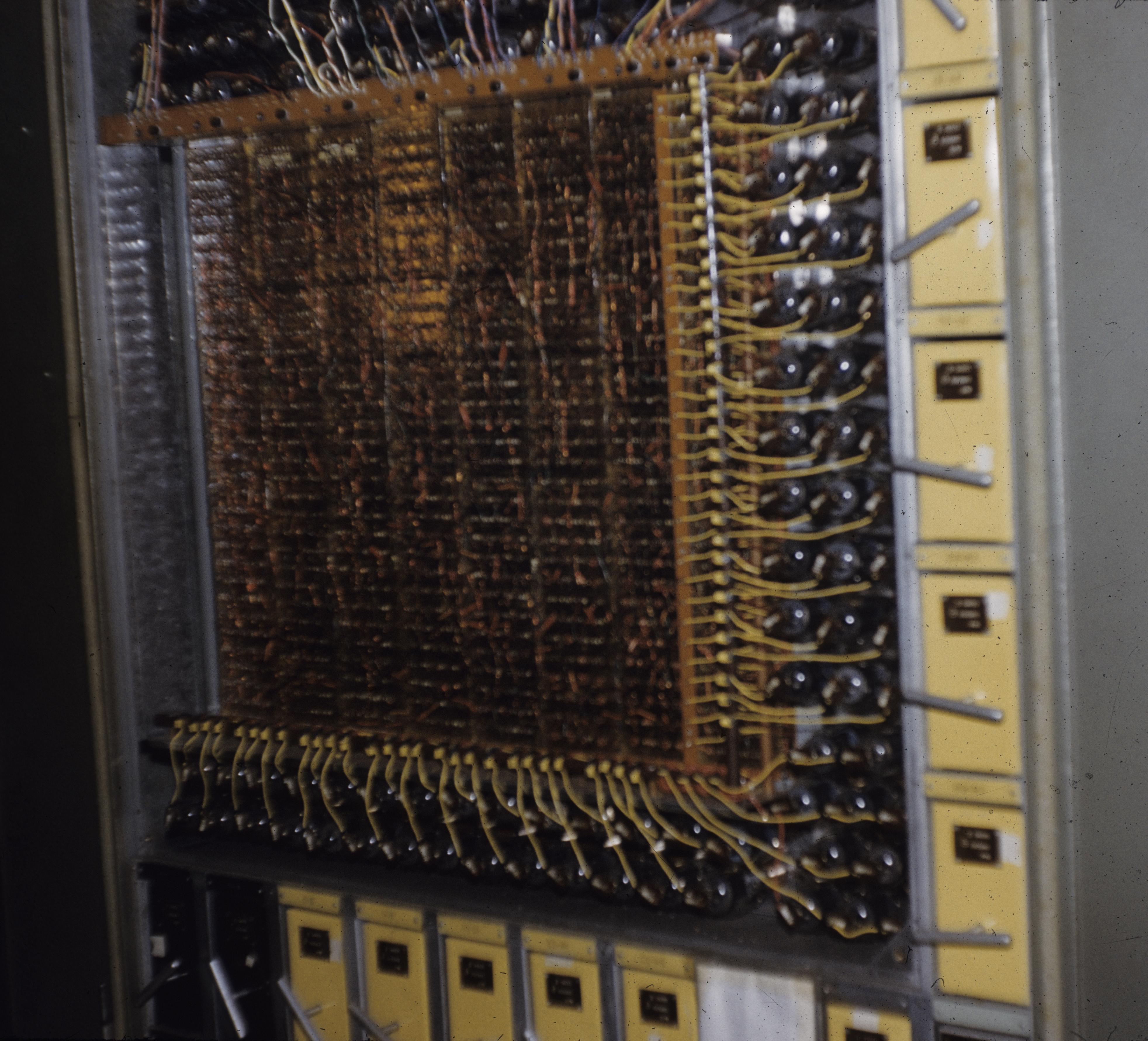
32x40 primary store coincident current address-decoding matrix.
Renwick's design for the primary store used two layers of ferrite core. The first layer stores no data and just acts as a coincidence gate. The second
layer stores data. It has been noted CITATION NEEDED that the induced signal in the sense wire through the first layer has desirable properties
for automatic write-back, but as stated above, EDSAC-2 implemented write-back independently as a separately microcoded step.
The mutable storage (RAM) capacity needed was 1024 + 256 = 1280 words of 40 bits. This is composed of the first quarter of the
reserved store, that was scratchpad, and all of the free store. (A location-by-location description of the role of this scratchpad is given in GJD and XXX).
An address-decoding matrix of dimensions 32x40 gives the required 1280 outputs.
Each single core in the 32×40 matrix acted as the physical gatekeeper/driver for one single 40-bit word line in the second layer.
The Science Museum photo appears to show the address decoder has 32 top-cap tubes along the left - possibly EL36 or PL36 pentodes.
Each has a 10-ohm resistor in series with its anode drive to the matrix. These resistors are shunted with a speed-up/precompensation capacitor.
Along the right margin is a fuse and a neon bulb for each row.
Along the bottom can be seen the valve bases for 40 column drivers. Again each has the 10 ohm resistor and capacitor parallel combination
in series with its output. These look as though they are soldered to the bottom of valve base
with the tube itself would be on the other side. More likely they are again connected to the anodes.
A close inspection of the actual artefact should confirm these
details by end of 2026.
NEW PHOTOS FROM WHIPPLE TO BE PUT HERE.
The 'fixed' store,
The fixed store was also commonly referred to as the 'reserved' or 'wired' store and the bottom
128 half-words were used as scratchpad (so it was not all really fixed).
This is explained by Wilkes (Annals 92 paper)
"These were, in fact, normal core planes, except that they had extra wires — which I will refer to as priming wires — threaded through some of the cores. When a current was passed through one of the priming wires, the cores through which that wire passed were magnetized in the direction corresponding to a 1. In a read operation, all cores in the word to be read were first set to 0. The priming operation was then performed and followed by a normal read operation. The primed cores delivered 1s and the unprimed cores delivered 0s There were four priming wires; which of them was used in a particular read operation was determined by the two high-order bits in the address of the word being read. One plane of the read-only memory had, therefore, the same capacity as four planes of normal memory."
The fixed store contains the initial orders, consisting of an assembler and loader for paper tapes, routines for input of numerical data, magnetic tape handling, a number of scientific functions (sin, cos, log, exp, RungeKuttaGill) and debugging and printing routines. It's content is loaded at address 0x200 and it starts with a jump table that is indexed with the operand to the 59 Order.
In the "Celebration of David Wheeler (1927–2004)" from The Computer Journal Vol. 48 No. 6, 2005 doi:10.1093/comjnl/bxh130, it states:
"Another example of Wheeler’s programming virtuosity was the
768-instruction fixed store for EDSAC 2, a read-only memory that
contained an assembly system and basic subroutines. The EDSAC 2 was the
first machine to use a microprogram, and Wheeler wrote that also. Both
had to be hand-wired onto magnetic cores. The fixed store routines
were then ‘potted’ in epoxy resin—a point from which there was no
return; they worked the first time and faultlessly."
Note that an alternative contemporary ferrite core ROM design was the Rope store.
This was used in the MIT Whirlwind project and the Apollo flight computers.
These weave the sense wires selectively to represent the data, but for EDSAC 2, Bill Renwick selectively wove the priming/address drive wires instead.
... describe here the routines that are not mentioned in the user manual ...
The GJD annotations reveal a routine for 'putting orders in the fixed store' that sounds very interesting ...
The 'main' store,
In mid life, (possibly November 1962) the architecture was augmented with the addition of the 'main' store and
an additional index register, RB, that provided one means of access to it. This was funded by a
£10,000 Nuffield Foundation grant.
The main store consisted of 16K words of ferrite core made by Ampex/Telemeter. Owing to the fixed address bus width
of 11 bits intrinsic to EDSAC-2 architecture, augmented with a desire to continue to use the pre-exisiting stores, the main store could not be fully or directly addressed
from the ISA. A combination of direct, indirect and indexed addressing was provided ...
A copy of David Barron's instructions for using the larger store are linked below. The first paragraph reads as follows:
"The MAIN STORE (so called to distinguish it from the existing
FREE and RESERVED stores) is a magnetic-core of 16,384 words. The
registers are numbered from 0 to 16383 (counting in ones, unlike the
free store).
Associated with the main store is a modifier register
b, which can count from 0 to 16383.
Orders are provided for setting, changing, and storing the content of this modifier,
but there are no conditional orders.
The main store can be used as a data store, or
it can be used to hold sections of program which must be transferred
to the free store before they can be obeyed.
Transfers between main store and magnetic tape must be made using a buffer in the free store:
a Library subroutine is provided to facilitate this.
Operation times are the same for the main store as for the free store."
DJG: please add a discussion as to whether a 'use main store' mode is needed owing to not being backwards-compatible, as we would could it today ...
EDSAC-2 Performance
EDSAC-2 ran one micro-order per cycle of the master clock. The master clock frequency had three settings, XX, YY and adjustable with
a variable capacitor ...
Modern Analysis
It is possible to compute the execution time of fixed-duration instructions by counting the micro-operations needed.
DJG's analysis of the OCR'd microcode gives the figures ...
Older Analysis
But some historic analysis is present in the DJW EPD folder of the Computer Lab Relics document store (classmarks being organised...)
Item: Durations of Orders and Operation Times
Cover page and three scanned pages.
1. DJW? Handwritten analysis
2. reverse side of sheet 1.
3. EDSAC 2 OPERATION TIMES DWB August 1961
The final sheet from David Barron (check) forms an interesting comparison regarding ... settling delays ...
EDSAC-2 Power Use
It is relatively easy to compute the static power
consumption of the various sub-circuits commonly used
in EDSAC-2 using spice or back-of-envelope computations.
We also have the power measurements from 1958 shown below.
The 'standard logic' circuits used in CT1, CT2 and CT3 for
register bits are repeated many times, so an analysis of their power use
is worthwhile.
Standard Flip-flop used in Chassis CT1-CT3 and elsewhere.
The standard AT7 triode flip-flop, that is used for each bit of the principle registers, is buffered and level-shifted with an AU7 cathode
follower.
A 'back-of-envelope' power estimation proceeds as follows.
The AT7 operates from 150 volts with a 10K anode resistor, no cathode resistor and can be naively assumed to drop 50
volts when ON and to have negligible leakage when off. Hence it takes 10 mA and consumes 1.5W, excluding heater power. There is
also some power consumed by the grid potential dividers, averaging 400V over 331K which consumes 0.5W. These power figures should
be doubled to include both halves.
The standard AU7, differential output buffer runs between +250V and -150V with 15K cathode resistors and a negligible 100R anode
resistor. The grid to cathode drop for AU7 is often quoted as -8.5V. The grid voltage for the OFF triode is -300 + 240/(91+240)
* 350 = -46 volts. For the ON triode, ignoring grid-to-cathode clamping current, will be -300 + 240/(91+240) * 450 = +26 volts,
which will saturate nicely, but not melt the grid. Elsewhere (e.g. in the adders) we can see clamping diodes that limit logic
outputs to the range -12 to 0 volts. Anyway, the cathode follower is approximately dropping a current of about 150V/15K through a
potential of 250+150=400V which is a power of 4W for each side.
Hence this estimate gives the total power per register as the heaters power for two double triodes (say 2W
each) plus 2 x (1.5 + 0.5 + 4) giving 16W.
The 'take up' gates that load a new value into a bit will not consume much
power (beyond heater power) when not in use (actively jamming in new data),
since only leakage current should flow.
Logic levels: Spice Simulation of E' and One Flip-flop
The simulation of one bit shows the flip-flop plates swinging between 87V and 135V whereas I'd used 50 and 150 in the rough analysis just above.
This means the flip-flop drops a mean current of (150-(87+135)/2)/10k per side through 150 volts, giving a static power of 2(150*0.0039) = 1.2W.
The shared 100R anode resistor of the output follower drops a steady 2 volts, meaning the total follower static power is 20mA * 400V giving 8W.
We also note the followers shift the voltage up by about 11 volts w.r.t. the flip-flop grids, giving logic levels at the interconnect of +12V and -6.
Although many signals are routed differentially throughout EDSAC-2, they are sometimes used single-endedly (e.g. in the
binary-to-unary diode decoders), with the other polarity being available meaning that inverters are never needed. The logic 1
level of +12V was presumably fairly reliable, owing to the clamping action from the grid-to-cathode diode of the flip-flop stage,
with variation arising mainly from the amount of shift in the followers. But where data is transferred between register bits,
these 'take-up' structures are differential.
Note that special
variants of some valves were made available for saturating computer use ... citation needed ...
"The 5963 or 7044: these are special-quality variations of the ECC82 specifically
engineered with chemically modified cathodes to resist "cathode
poisoning" when left sleeping in a cut-off state for long periods." says Gemini.
I have no record of these explicitly being deployed for EDSAC-2. I can read the part numbers of the chassis we do have ...
A pseudo ground, E', is used in a number of places. I must simulate that with spice to see what it does - presumably noise margin improvement or supply-voltage-variation tracking rejection ...
SPICE simulation of one generic CT1-3 register flip-flop with its cathode-follower buffer.
Power Rails and Standard Connections
One of the folders or sections in DJW26 has detailed circuits for electro-mechanical (relay) power supply sequencing. I've not looked
at it much yet, but I don't think it contains the main power supply schematics themselves. (The power supply schematics for the
magnetic tape unit are in the portfolio somewhere ...)
Standard power chassis pin connections and variants
Chassis pins 1 through 19 implement the standard supply connections
common to all chassis, with 18 through to 24 being allocated on a per-chassis basis.
The majority of 'common logic' runs on the +150v and -150v rails (true for CT1?).
These two rails have the highest reported current usage.
A common design pattern is to run RVL (resistor-valve logic) between these two rails with minumum earth current. Cathode followers ....
Note 1: The signal E' appears variously. It is possibly a temperature-compensated pseudo earth potential.
Note 2: The discriminator level was presumably set on a pot and is used in the sense-wire comparators to adjust common mode? or is it absolutely? Need to check. And what is 1L and -1L?
DJG notes about the EDSAC-2 supply rails:
1.E
Ground
2-4, 8-10
Heaters
5. -6M
6. -165M
7. +300
11. -300A
12. -300B
13. +150
Common logic
14. +100
15. +50
Clamp driver bias CT5
16. -150
Common logic
17. -300
19. +250
Core store driver (CT5),
21. -450
CT9 and CT12: logic level clamping
22. -150A
CT3, CT5-6 and CT11
Reset
23. -150B
CT3 and CT11
sequencing?
24. -12V
CT1-5, CT10-12: logic level clamping
From the way some flip-flops use the -150A as grid bias for one
side and -150B for the other side (eg. matrix driver units in
CT6), I guess these two may have been switched-on or strobed in a specific sequence to achieve a system reset.
Supply pins 5 and 6 have strange names/designations. We see they are used in CT8 (control matrix bias amplifiers) for the anode supply of the first stage. Must find out more!
There is no doubt that EDSAC-2 used a lot of electricity. A page of measurements is included in the DJW26 portfolio (reproduced below).
Looking though the schematics, EDSAC-2 used a variety of different valves, with most logic being implemented using 12AU7 and 12AT7 double-triodes. But heavier current drive to the microcode ROM, core store and punch often uses CV4062s or A2134s as cathode followers.
EF91s are used to amplify diode-logic and core sense wire signals. Other valves, like EL82s are
used to drive the CV4062 grids.
[More powerful valves are positioned outside the pluggable chassis set: they are
around the edges of the microcode matrix and the primary store coincidence decoder. The circuits for these are not in the portfolio
but I may learn the valve type and reverse engineer the circuit after a forthcomming visit to the Science Museum store.]
The 12AU7/AT7 value has a standard heater power of 6.3v at 300mA =1.9 watts, but
it may be they were under-volted to extend lifetime. If the average anode
current was 10 mA through a 150 volt circuit, the static power would be 1.5 watts.
Each full-length chassis is typically punched to accommodate 36 nine-pin valves, but these are not always fully populated.
With between 50 and 60 valves on a full-length chassis, each consuming
about 3 watts and with about 140 chassis, this give a back-of-envelope power estimate
of 23 kW. This includes the tape store amplifiers and logic but not its motor currents.
DJG: I shall count up the valves present on each chassis to come to another figure. I can also work out the DC
conditions and estimate the static power use for each flip-flop and driver.
Power use measurements logged in October 1958
October 1958 power measurements imported into a spreadsheet
Some EDSAC-2 programs and an EDSAC-2 emulator coded in python: Geoff Daniell mounted his GJD EDSAC-2 archive online on plussnet. This contained a folder of programs that I have hosted here: gjd_edsac2_sample_progs.zip.
There does not seem to be a copyright notice associated with it. I will check with him over the copyright status.
"PROGRAMMING FOR EDSAC 2 WITH MAIN STORE", D. Barron, November 1962 PDF.
(C) CC4BY 2026 DJ Greaves, University of Cambridge.


 PDF
PDF