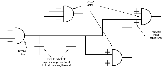
The figure shows a typical net, driven by a single source. To change the voltage on the net, the source must overcome the stray capacitance and input loads. The fanout of a gate is the number of devices that its output feeds. The term fanout is also sometimes used for the maximum number of inputs to other gates a given gate is allowed to feed, and forms part of the design rules for the technology.
To estimate the delay from the input to a gate, through the internal electronics of a gate, through its output structure and down the conductor to the input of the next gate, we must add three things:
The propagation delay down a conductor obeys standard transmission line formula and depends on the distributed capacitance, inductance and resistance of the conductor material and adjacent insulators. For circuit board traces, resistance can be neglected and the delay is just the speed of light in the circuit board material: about 7 inches per nanosecond, or 200 metres per microsecond.