
| Title: | Use of the teaching board | |
| Number: | 21 | |
| Author: | Richard van der Hoff | |
| Date: | 25 August 1999 |
This memo documents the use of the assembled teaching board. Much of this is also described in lab 1.
The teaching board is actually composed of three circuit boards. The one in the left of the box is the Altera board; the one one on the right is the ARM board, and the board underneath links them together and provides a power supply, and optionally an SRAM chip.
The Altera board has two Programmable Logic Devices; the foremost one is called the MAX, and has been programmed to provide an interface between the ARM and the FLEX, to prevent damage to the ARM. The rearmost one is the FLEX, and may be programmed freely by users. To do this it is neccessary that the jumpers on the board be set correctly - from the rear of the box, they should be to the left, left, right and right.
In order for the boards to work correctly, all three connections (power, parallel data to the Altera board, serial data to the ARM board) must be made to the computer. Some of the boards may also have a power switch - this is a big switch on the power cable. The FLEX may then be programmed using the MAX+plus software as an EPF10K20RC240-4, and the ARM board may be programmed using either of the ARM debuggers.
Here is a schematic of the patch board as a postscript file, and as a PDF.
The patch board and MAX software have been designed in such a way as to provide all of the signals from and to the ARM necessary to use the FLEX as a memory-mapped device. All signals, except /WAIT and INT4, pass through the MAX and through resistors, to prevent damage to the chips caused by programming the FLEX incorrectly.
The MAX operates in one of two modes, selectable by the leftmost DIP switch, and indicated by the decimal point of the leftmost digit display. With the switch down, the MAX acts as a bidirectional buffer, allowing the ARM and FLEX to communicate. In this mode, the LED is lit.
On two of the signal lines (D0 and /OE), the MAX has inputs from the FLEX side of the resistor which allow it to sense if the line is being pulled in opposite directions - if this is the case, the MAX will turn off all of its outputs and display "Er" (for error) in the LED segments. Pressing the ARM reset button clears this condition (as well as restarting the ARM, of course).
The other mode, with the switch up, turns off all of the MAX's outputs, so that the FLEX or ARM may be used individually without concern of them damaging each other.
Switch settings for the MAX chip
Switch Setting SW0 Up Flex & ARM isolated Down Flex & ARM connected Memory timing cycle diagrams
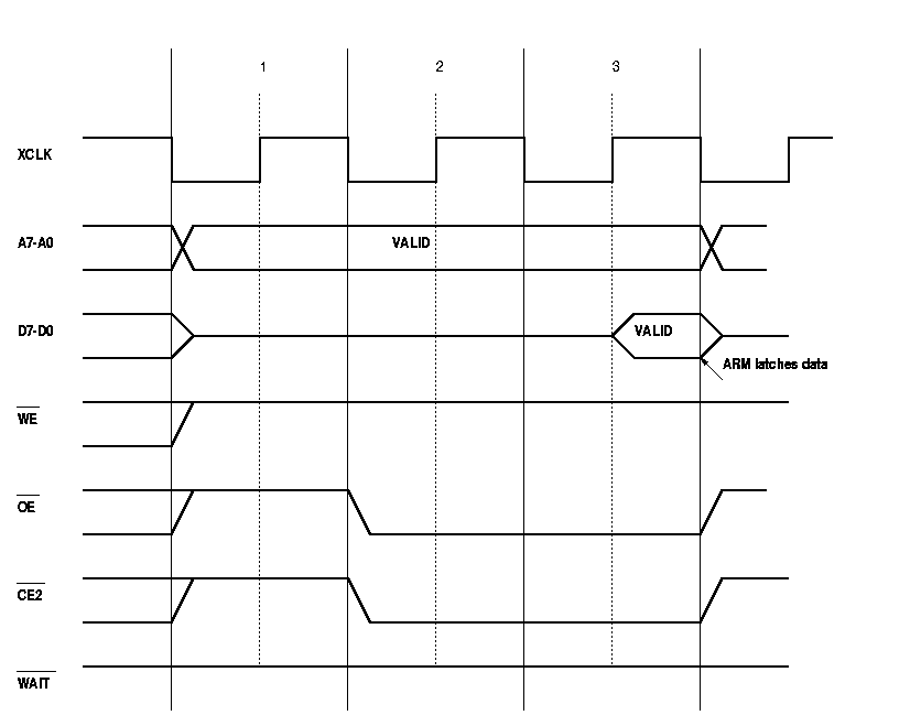
ARM reading from FLEX
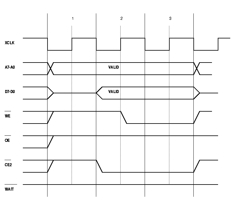
ARM writing to FLEX
Testing
There are two commands in the ARM EEPROM that can be used for testing the connection. They can be accessed by connecting to the board directly down the serial line, e.g. by using Hyperterminal, and rebooting the board.
- Meminfo
This displays the curent configuration of the memory controller. Normally, there should be an entry for the Altera board at 0x8000000 using CE2 here.
- iotest
When used in conjunction with the correct FLEX program, this tests the connection between the boards. It displays its result on the LEDs of the ARM board. It should briefly cycle through digits on the FLEX display, then trip the error detection system on the MAX and reset the ARM LEDS to their normal state.
It must be noted that, by default, pins on the FLEX are logic low. If it is intended to connect the FLEX and the ARM, all pins named ARM_... below must be assigned in the .acf, and declared and defined in the list of ports to the top-level module.
The pin assignments to the FLEX are as follows:
Signal I/O/B Pin Header Connection CLK (25.175MHz) I 91 - XCLK (24 MHz) I 211 A14,B14,C14 /LEDA0 O 6 - /LEDA1 O 7 - /LEDA2 O 8 - /LEDA3 O 9 - /LEDA4 O 11 - /LEDA5 O 12 - /LEDA6 O 13 - /LEDA7 O 14 - /LEDB0 O 17 - /LEDB1 O 18 - /LEDB2 O 19 - /LEDB3 O 20 - /LEDB4 O 21 - /LEDB5 O 23 - /LEDB6 O 24 - /LEDB7 O 25 - /PB1 I 28 - /PB2 I 29 - SW0 I 41 - SW1 I 40 - SW2 I 39 - SW3 I 38 - SW4 I 36 - SW5 I 35 - SW6 I 24 - SW7 I 33 - MOUSE_CLK B 30 - MOUSE_DATA B 31 - VGA_RED O 236 - VGA_GREEN O 237 - VGA_BLUE O 238 - VGA_HORIZ O 240 - VGA_VERT O 239 - ARM_A0 I 222 C48 ARM_A1 I 221 C47 ARM_A2 I 220 C46 ARM_A3 I 219 C45 ARM_A4 I 218 C44 ARM_A5 I 217 C43 ARM_A6 I 215 C42 ARM_A7 I 214 C41 ARM_D0 B 231 C56 ARM_D1 B 230 C55 ARM_D2 B 229 C54 ARM_D3 B 228 C53 ARM_D4 B 227 C52 ARM_D5 B 226 C51 ARM_D6 B 225 C50 ARM_D7 B 223 C49 ARM_/CE2 I 208 C40 ARM_/WE I 207 C39 ARM_/OE I 206 C38 ARM_/WAIT O 181 C16 ARM_INT4 O 175 C15 RAM_A0 O 201 C34 RAM_A1 O 200 C33 RAM_A2 O 199 C32 RAM_A3 O 198 C31 RAM_A4 O 196 C30 RAM_A5 O 195 C29 RAM_A6 O 194 C28 RAM_A7 O 193 C27 RAM_A8 O 46 A16 RAM_A9 O 48 A17 RAM_A10 O 50 A19 RAM_A11 O 49 A18 RAM_A12 O 192 C26 RAM_A13 O 45 A15 RAM_A14 O 191 C25 RAM_D0 B 202 C35 RAM_D1 B 203 C36 RAM_D2 B 204 C37 RAM_D3 B 190 C24 RAM_D4 B 188 C23 RAM_D5 B 187 C22 RAM_D6 B 186 C21 RAM_D7 B 185 C20 RAM_CE O 182 C17 RAM_OE O 183 C18 RAM_/WE O 184 C19 Key
LEDA0..7 Left-hand digit LEDB0..7 Right-hand digit PB1..2 Push buttons SW0..7 DIP switches MOUSE_ Signal to 6-pin mini-DIN connector VGA_ Signal to 15-pin D connector ARM_ Signal to ARM board, via resistors & MAX RAM_ Signal to RAM connector. Note RAM_CE and RAM_OE pass through inverters. CLK 25.175MHz clock XCLK 24MHz clock, as used by the ARM I Input to FLEX O Output from FLEX B Bidirectional signal / Indicates an active-low signal
Assignments of unused programmable pins on the FLEX
FLEX pin Header pin 51 A20 53 A21 54 A22 55 A23 56 A24 - 61 A25 62 A26 63 A27 64 A28 65 A29 66 A30 67 A31 68 A32 - 70 A33 71 A34 72 A35 73 A36 74 A37 75 A38 76 A39 - 78 A40 79 A41 80 A42 81 A43 82 A44 83 A45 84 A46 - 86 A47 87 A48 88 A49 - 94 A50 95 A51 - 97 A52 98 A53 99 A54 100 A55 101 A56 Connector B 109 B15 110 B16 111 B17 113 B18 114 B19 115 B20 116 B21 117 B22 118 B23 119 B24 120 B25 - 126 B26 127 B27 128 B28 129 B29 - 131 B30 132 B31 133 B32 134 B33 - 136 B34 137 B35 138 B36 139 B37 - 141 B38 142 B39 143 B40 144 B41 145 B42 146 B43 147 B44 148 B45 - 151 B46 152 B47 153 B48 154 B49 - 156 B50 157 B51 158 B52 159 B53 - 161 B54 162 B55 163 B56
Memory map
The EEPROM on the ARM board has been programmed to set up the following memory map on reset:
Start End Size User Access Width CE lines Wait States Description 00000000 000007FF 2KB RW - - 0 Internal SRAM 00000800 0001FFFF(B)
0003FFFF(C)128KB(B)
256KB(C)RW 16 bit CE1 1 On-board RAM 04000000 0403FFFF 256KB RO 8 bit CE0 3 EEPROM 08000000 0BFFFFFF - RW 8 bit CE2 1 FLEX FFFF0000 FFFFFFFF - RW - - - Control registers Other - RW 16 bit CE5 0 - Key
The revision is given by the last letter of the ASSY number.
(B) Revision B boards only (C) Revision C boards only References
LH77790A/B user guide
AEB welcome guide
AEB users guide
AEB Technical Help
Revision B Schematic
Revision C Schematic