DRAMs for use in PCs are mounted on SIMMS or DIMMS, but for embedded applications, often just soldered to the main PCB. Normally one bank of DRAM is shared over many sub-systems in, say, a mobile phone.
SoC DRAM compatibility might be a generation behind workstation DRAM: e.g. using DDR2
Typical DRAM pin connections:
|
|
High bandwidth: 64 bits times 400 MHz giving 25.6 Gb/s peak.
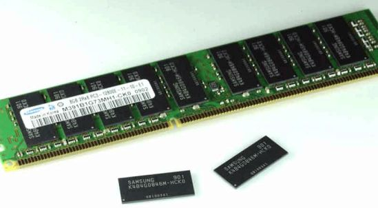
High capacity: Example 1 Gbyte DIMM made of 8 chips.
High latency: 20 clock cyles access time to a closed bank. Worse if a bank is already open at the wrong place.