A multimedia workstation based on a DAN has been largely completed. This is a demonstrator of the architecture and provides a test-bed for its exploration. To show the feasibility of DAN devices and to investigate their properties, a camera node and a DSP node have been built. A framestore node has been designed and until the hardware is complete is being emulated by a DECStation 5000/25. To investigate the use of the DAN as a processor-memory interconnect, in addition to its use for interconnecting multimedia devices, a CPU and memory node have been constructed.
The demonstrator is based on the Xilinx FPGA based switch element designed for the Fairisle ATM LAN [\bf\protect\citenameLeslie91] and is therefore constrained to an 8 bit wide data path and a 20MHz clock rate, providing nominally 160Mbps full duplex per port. It seems likely that custom ICs and possibly a wider data path would be used in a full DAN implementation. The complexity of the interface hardware is comparable to that required for implementing the base SCI protocols for which high speed VLSI implementations have been produced in both GaAs [\bf\protect\citenameNodeChip92] and CMOS [\bf\protect\citenameNodeChip93].
The ``network interface'' of a DAN based machine is simply a cell router from the internal interconnect to the LAN. It is very similar to a port controller (or line-card) of an ATM LAN switch. However, being at the machine-network interface it is also the barrier to the outside world and will need to implement security (e.g. drop cells with bogus VCIs) and data-flow control.
The demonstrator network interface uses the port controller that was developed for the Fairisle ATM switch [\bf\protect\citenameLeslie91]. This has minor software modifications, but the hardware is identical, and it performs very similar queuing in the DAN as it would in a switch. This supports full duplex operation at 100Mbps between the network link and the internal interconnect. More details on the performance of this device has been described in [\bf\protect\citenameBlack94].
The network interface node is the boundary between the DAN with its simplifying reliability property, and the LAN where more complicated protocols must be used for error detection etc. As streams cross the boundary into the DAN, for example, complete AAL5 PDUs could be assembled and the CRC checked. By doing this it is possible to ensure that only complete and uncorrupted PDUs are let onto the DAN, and that they are within their resource allocation (e.g. mean and peak data rates). This can remove the need for complicated reassembly, error detection, and protection mechanisms on individual nodes in the DAN.
The ``ATM camera'' is a device which captures and digitizes real-time video into an ATM cell stream. Two versions of the camera have been produced and both are described as they show examples of ``dumb'' and ``supervised'' devices.
The first version of the camera was completed in April '92. As an example of a ``dumb'' device, it shows how simple a DAN node can be.
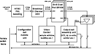
Figure 1: Datapath diagram for DAN Camera V1
The node contains no processor and is controlled via a single cell message that it receives on a fixed VCI. The cell configures parameters such as the ``grab'' window, scaled size, colour mode and output VCI. This control cell is generated by a manager process running on a processor node. The manager exports an RPC like interface to clients. Multiple clients can connect to the manager and request different video streams on different VCIs. The process will deal with scheduling the different requests and sending the appropriate configuration cell to the camera. Note that the video data is never touched by the management process.
Additionally, format conversion processes can be inserted into the stream of video data. In particular, a process that converted V1 camera video into Pandora [\bf\protect\citenameHopper90] format was demonstrated as part of the software emulation of a Pandora Box described later.
The V1 camera digitizes in either 8, 15 or 24 bits RGB into a 2 line buffer. This provides decoupling between the video and network clocks. The cells composing each line of digitized video are preceded by a cell containing a line number and frame count.
With only a 2 line buffer, this type of camera generates very bursty
traffic. A typical application might require a 352x288![]() 24bit RGB picture at
15 fps. This requires a continuous rate of 36Mb/s. However, the V1
camera with its 2 line buffer will generate bursts of over 130Mb/s
during active areas of the frame. The availability of inexpensive
``video fifos'' (used to provide freeze frame capability in VCRs)
allowed this problem to be overcome in the version 2 camera. By
buffering an entire video frame, transmission at the mean rate can be
achieved.
24bit RGB picture at
15 fps. This requires a continuous rate of 36Mb/s. However, the V1
camera with its 2 line buffer will generate bursts of over 130Mb/s
during active areas of the frame. The availability of inexpensive
``video fifos'' (used to provide freeze frame capability in VCRs)
allowed this problem to be overcome in the version 2 camera. By
buffering an entire video frame, transmission at the mean rate can be
achieved.
The video format was also changed for the V2 camera. It was decided to package the video in multiples of 8x8 pixel tiles. This has a number of advantages over line based methods: having a fixed minimum unit is useful for hardware implementations - by making this unit 64 pixels in an 8x8 block we do little to restrict the range of possible picture sizes; two dimensional blocks are also the basis for many image compression schemes - 8x8 blocks were chosen for both JPEG and MPEG, so our tiled video scheme lends itself well to compression with these methods. Were the DAN interface to be built into a CCD controller, the 8x8 tiles could be read directly from the CCD element, avoiding the scan line to tile conversion that is necessary when dealing with conventional video formats designed for display on CRTs.
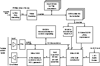
Figure 2: Datapath diagram for DAN Camera V2
While the camera V1 was a ``dumb'' device, the second version of the camera uses a simple 8-bit microcontroller to provide more complex control functions; for example, it is possible to download a schedule which is repeatedly executed, which defines for each video field which video source to use, the XY resolution required, depth, coding (RGB, YUV, JPEG), and destination (i.e. VCI).
The audio node [\bf\protect\citenameAtkinson93] is designed both to provide audio I/O
to the DAN workstation, and to be available as a general signal
processing node![]() . A CODEC provides
stereo audio capture and playback in a number of common rates and
formats up to stereo 48kHz 16 bit PCM (DAT format). The CODEC feeds an
Analog Devices 16bit integer DSP which connects to the DAN via 4k of
dual ported SRAM and a control Xilinx FPGA.
. A CODEC provides
stereo audio capture and playback in a number of common rates and
formats up to stereo 48kHz 16 bit PCM (DAT format). The CODEC feeds an
Analog Devices 16bit integer DSP which connects to the DAN via 4k of
dual ported SRAM and a control Xilinx FPGA.
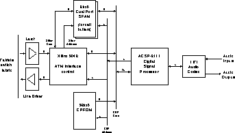
Figure 3: Datapath diagram for DAN DSP/Audio node
Half of the dual ported memory contains a FIFO queue of cells received from the DAN. Arriving cells are presented to the DSP which must explicitly free the cell buffer before it is reused. If there are no free cells then the DAN interface refuses incoming cells providing back-pressure to the source.
A further queue is used for cells to be transmitted across the interconnect. However, cell buffers on this list may come from anywhere in the SRAM. This allows the DSP to process cells in situ in the receive buffer, and then thread them back on the transmit queue. This leads to efficient stream processing without data copy. Since the threading operation consists of a single write to the SRAM and a small amount of internal bookkeeping the 12MHz DSP can perform the null operation (i.e. simply forwarding the data) at more than the 160Mbps interconnect rate.
The DSP node falls into the ``supervised'' class of devices, since the DSP processor can perform some simple management functions. However, like the camera, the card is again optimised for the data path and most control functions are delegated to a general purpose processor node.
This section describes the final design of the DAN framestore which was arrived at after evaluation of various levels of functionality using software emulation on a DECStation 5000/25. Section 4.4 describes the opposite extreme of implementing the complete windowing system in the framestore.
The DAN Framestore performs a single rendering operation, that of taking a number of 8x8 pixel tiles from within an arriving PDU, and copying them to the display. The VCI of the incoming cells identifies the destination window, and the associated VC context contains parameters such as the position of the window on the display, and the pixel format (e.g. 8 bit mono, RGB 3:3:2, RGB 8:8:8).
While the hardware version of the DAN framestore will support simultaneous display of windows with different depths, the frame buffer in the DECStation is only 8 bits deep so most formats require conversion in software before display.
Due to the reliable nature of the DAN, reassembling complete PDUs can be avoided, and the data contained in the incoming cells copied directly to the framebuffer. In the case of video streams from remote sources, the network interface node can ensure that only complete and uncorrupted PDUs are let onto the DAN. While dropping corrupt PDUs will result in small areas of the picture not being updated, inter-frame correlations often make these hard to detect.
The framestore does not provide explicit support for more traditional rendering operations, such as drawing lines and displaying text. Such operations are performed on a processor node. This has a local pixel map and can generate the list of modified tiles as it renders into this map. Any of these video differences which are in a visible region of the window are sent to the framestore for display. This minimises the number of primitives which must be supported by the framestore, simplifying hardware implementation, and also has the benefit of making video and graphical windows indistinguishable.
Clipping of windows is performed on a per-pixel basis by the DAN Framestore. Each client, communicating on a separate VCI for each window, is offered a ``virtual write-only display'' abstraction. This obviates the need for a shared service in the display datapath to enforce protection barriers, and simplifies the process of resource allocation by preventing ``QoS Crosstalk'' between applications - the resources used by each application for rendering its windows are naturally accounted to that application process rather than being some unknown proportion of the shared service.
Clients are responsible for all updates to their own windows, though for most applications a shared library with a set of default rendering operations will be indistinguishable from the more conventional server-based approach. Clients with more specialised needs are free to implement their own rendering policies. For example, a client may delay flushing updates of large amounts of text to the framestore until it believes that no more output will be received for a while.
Clipping is achieved using an overlay plane to hold a tag for each pixel. Each window (and corresponding VCI) is also allocated a tag. Each incoming pixel on a particular VCI is only copied to the framebuffer if the tags are identical. The tag space is relatively small and is allocated using a map colouring algorithm. This method allows both video and graphical windows to be clipped against each other to arbitrary boundaries; a useful feature often unsupported by other multimedia peripherals.
The software emulation on the DECStation proved capable of clipping a number of arbitrary shaped video and graphical windows against each other with very little loss of performance, the main bottleneck proving to be the speed at which the processor was capable of draining the receive FIFOs of the ATM interface.
The processor node developed for the DAN [\bf\protect\citenameHayter93] allowed investigation of two areas: the use of the interconnect to carry CPU-memory traffic and to allow processing to take place on multimedia data types. It is noticeable that in many existing systems multimedia data are second class, the only operations that can usually be performed in real-time are capture, replay and presentation. Where other processing is done it tends to be performed by specialised hardware; for example compression/decompression of video. The DAN processor node aims to provide high speed access to such data and hence permit more general processing on these data.
The DAN processor node consists of an ARM600 chip, composed of the ARM6 processor core, MMU, primary cache and write buffer, and a large external secondary cache (256kbytes in 32 byte cache lines). The secondary cache is normally configured as two way associative with LRU replacement, but may also be set as direct mapped. On a miss the external cache controller sends a single cell request to a memory server, and receives a single cell reply containing a line of data. The secondary cache is copy-back, and if data needs to be flushed it may be piggybacked onto the request.
Two different memory servers were implemented for experimentation with cache line transfers across the DAN. The most commonly used one was implemented in software on a Fairisle port controller, as this enabled simple recording of addresses and data transfers during experiments. The second server was implemented in hardware and demonstrated the expected two cell response time but has not been widely used as it is less useful from an experimental point of view.