Extracting a 3DES key from an IBM 4758Part 4: How the DES cracker worksThe basic idea of a brute force "DES cracker" is to try all possible keys in turn and stop when one is found that will correctly decrypt a given value into its plaintext. Sometimes, as in problems we have been tackling, the plaintext that we need to match is known (we often use all zeros) and sometimes the correct decryption can only be determined statistically (for example, in the RSA challenges posed in the late 90s, the value looked like English text). This cracker design actually works the other way round; viz it takes an initial (zero) value and encrypt it under incrementing key values until this output matches the encrypted value we seek. The design runs at 33MHz ie: it tries 33 million keys per second. This might sound fast, however this is rather slow for cracking DES keys - and it would take, with average luck, about 34.6 years to crack a single key. So we arrange to crack up to 16384 keys in parallel (ie: we have available the results of encrypting zero with 16384 different DES keys and we check against all of these at the same time). It would still take nearly 70 years to be sure of cracking all of them - but during that 70 years one would have, on average, have been cracking one key every 37 hours and one would expect, with average luck, to find the first key after about 25 hours. (For the detail of these sums have a quick peek here). Since cracking just one key is of use to us in our attack on the IBM 4758, we need only consider waiting about a day for results.. so our design is of real practical use. As an aside, you may be wondering why we choose to crack exactly 16384 keys in parallel. Cracking more would speed things up -- but unfortunately on the system being used there is only 256K bits of memory available to hold the encrypted values and 16384 values is the most that this will hold. 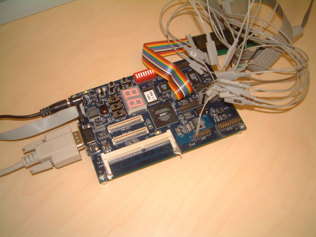
Our DES cracker uses the Altera NIOS Development board described earlier. This board contains an APEX EP20K200EFC484-2X FPGA chip1 which contains 8320 Logic Units (LUTs) which can be viewed as being equivalent to approximately 200,000 logic gates. The FPGA is programmed with a DES cracking design alongside of which, within the FPGA, is placed a 16-bit NIOS processor. The NIOS processor runs a simple program (written in C and loaded into some local RAM on the FPGA) which looks after a serial link. The values for the DES crack are loaded down the serial link, and when results are obtained they are sent back this way. This diagram shows the general arrangement: 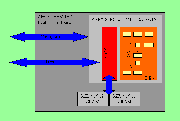
In a software version of DES you'd use the same variables for each round and a "for loop" such as:
	for (i=0; i<16; i++)
	{
		ShiftAndRotate(key);
		temp = R;
		R = L ^ DESfunction(R, key);
		L = temp;
	}
For the hardware DES cracker a pipelined version of the algorithm is used: 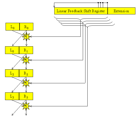
At each clock interval, all of the LR pairs are moved down into the next set of registers. Therefore, after an initial start-up period of 16 clocks, results appear from the end of pipeline at the clock rate of 33MHz. The key values are not pipelined from stage to stage along with L and R. Instead a Linear Feedback Shift Register is used, which is extended to the right of its actual 56 bits so as to record older values of the key. These can then be statically connected, in an appropriate manner to the various pipeline stages. This space-saving technique was previously used by Hamer and Chow in their Transmogrifier DES cracker design 2. In order to determine whether there is a match to one of 16384 values, the value is "hashed" down from 64 bits to 14 and this gives the RAM address to be consulted. If the value at this RAM address matches the entire value then the crack is finished. Otherwise, the system continues. A tedious complication is that the Altera board has a limited amount of RAM on board, just two SRAMS each 32K by 16 bits. This means that the 64-bit compare has to be done in two 32-bit halves. If the first half matches (as happens every few seconds) then the pipeline is suspended and the second half of the value is checked. You can see this happening on this logic analyser picture below. The regular signal on the third line is the clock. The second signal down shows a 32-bit match is occurring. This causes a STOP of the pipeline (top signal) and access to an odd numbered address value (bottom signal). The other signals are some of the data and address lines. 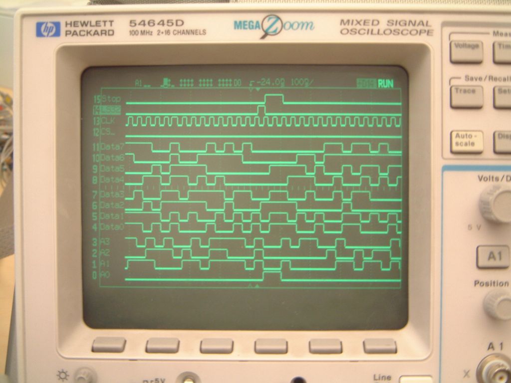
Next part: How the attack works
Links1 APEX 20K Programmable Logic Device Family Data Sheet http://www.altera.com/literature/ds/apex.pdf 2 Ivan Hamer and Paul Chow. "DES Cracking on the Transmogrifier 2a" Cryptographic Hardware and Embedded Systems, LNCS 1717, Springer-Verlag, 1999. pp 13-24. http://www.eecg.toronto.edu/~pc/research/publications/des.ches99.ps.gz |